In the modern electronics manufacturing industry, PCB design is a crucial phase. A well-thought-out and precise PCB design not only enhances circuit performance but also reduces production and maintenance costs. To assist you in designing PCBs that are suitable for assembly, this article will share some key tips on PCB design.
Before delving deeper, let's first discuss PCB assembly and PCB assembly design.
There is an issue that experienced PCB design engineers tend to encounter less frequently but is common among newcomers. It is the failure to fully consider assembly during the initial circuit board design phase, where more attention is focused on the PCB itself without a comprehensive understanding of how the circuit board should be used in the product or application. Neglecting PCB assembly can result in a series of concurrent issues.
When viewed individually, the circuit board design may seem entirely acceptable, but certain design decisions can make future assembly challenging. For example, components may be placed too close to each other, leading to potential issues with the subsequent product's operation or performance.
Component availability issues: If components are unavailable, the entire manufacturing process may experience delays.
One of the most common issues raised by inexperienced PCB layout engineers is the spacing between components. Placing all components too close to one another can lead to various problems, which may necessitate redesign and remanufacturing, resulting in both time and cost losses.
Experienced PCB layout engineers employ various techniques to avoid spacing issues between components during the assembly process. For example, when designing component footprint, they create place_boundary (in Allegro), and the place_boundary is larger than the actual physical outlines of the components. This ensures that when placing components, there is always sufficient spacing between them. This approach helps decrease potential issues that may arise due to components being placed too closely together during the assembly process.
PCB layout engineers must carefully place components to prevent the overlap of place_boundary shapes for components.
Different types of components have varying spacing requirements between them. For example, the minimum spacing between discrete components like capacitors and resistors should always be at least 10 mils, with 30 mils being the preferred spacing. There are also additional spacing rules, as shown in the diagram below:
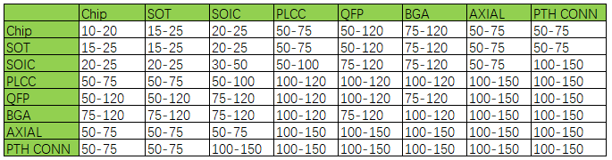
The above values may vary based on design constraints and the capabilities of assembly suppliers.
Experienced engineers choose their components early in the design phase to ensure minimal conflicts between design and actual assembly.
By considering component sizes from the outset, the PCB assembly process can proceed smoothly. Typically, smaller components occupy less space on the PCB, and PCB layout engineers can engage in discussions with circuit design engineers to explore the possibility of reducing component sizes, thereby creating additional space on the circuit board.
Under no circumstances should lead-free components be mixed with components not designated for lead-free assembly. If any component necessitates lead-free assembly and there are no viable alternatives for traditional leaded solder, the entire PCB must be subjected to lead-free assembly, and all components must comply with lead-free assembly requirements. This is a crucial step to ensure soldering quality and compliance, mitigating potential soldering issues and violations of environmental regulations.
During the layout phase, strive to evenly distribute large components to achieve as uniform a heat distribution as possible during the solder reflow process. Ensure that the assembly contractor customizes a heat profile unique to the reflow oven for each assembly job
Careful scrutiny of the components used in the design should occur early in the layout phase. If there is sufficient space on the PCB, and the current design does not necessitate the use of smaller footprint components, opting for larger components is more advantageous for PCB assembly.
For instance, consider using 0402 resistors whenever possible instead of 0201 resistors. If all requirements can be met with 0805 resistors, there is no need to select 1206 resistors, as this can reduce the overall size of the PCB.
Strive to avoid mixed manufacturing processes whenever possible. The benefits of a single through-hole component do not outweigh the additional time and cost involved. It is more efficient to use multiple through-hole components or none at all. If through-hole technology is employed, placing all through-hole components on one side of the circuit board will reduce manufacturing time.
The availability of components is closely tied to the delivery schedule of the final product. Engineers should check the availability of all components (inventory, lead times, and potential obsolescence) before commencing the design to mitigate this issue. If certain components have longer lead times, it's advisable to place advance orders.
The Bill of Materials (BOM) is a critical aspect of both design and assembly. If there are any issues with your BOM, the assembly facility may halt the project until the problems are resolved. One way to ensure the BOM remains up to date is to review it whenever there are changes in your design. When adding new components to the schematic while the layout is in progress, ensure that the BOM has been updated, including the correct part numbers, descriptions, and component values. During the design process, engineers may change components due to reasons such as long lead times, size, or availability, but they might forget to update the BOM with the new part numbers. This oversight can lead to various assembly issues and delays.
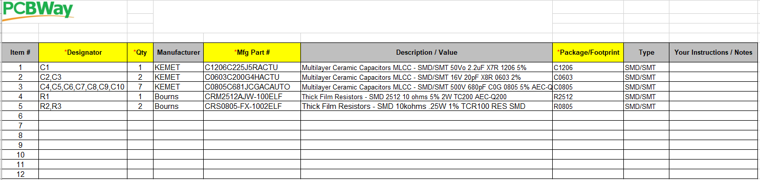
Prepare each bill of materials in the format of the following example to accurately identify all components to be assembled on each circuit board. A properly formatted BOM should contain the following columns:
Click to download PCBWay BOM Template
Certainly, it can also include the following information:
Component footprints are another significant aspect of layout design. PCB layout engineers must ensure that the footprints used on the board are accurately created according to the recommended pad patterns in the datasheets. Properly identifying the correct components and their corresponding pad patterns using the part number key in the datasheet is crucial. Misinterpreting the datasheet can result in incorrect footprints, which may necessitate a complete redesign and remanufacturing of the circuit board.
The following diagram illustrates a part number key and examples of various footprint types:

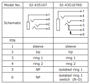
Please refer to our post on creating footprints in Allegro to learn how to design footprints.
A significant impediment during assembly arises when the silkscreen layer lacks essential markings such as Pin1 indicators, component polarity, or orientation. Please ensure that all critical instructional markings, including but not limited to designators, Pin1 markings, and polarity indicators, are included in the component footprints within the design. These markings are crucial for the proper assembly of the circuit board.
In circuit board design, ensuring that each connection of every component has its own independent pad is a crucial principle. This is done to ensure the reliability and performance of the circuit board, as well as to simplify the assembly and manufacturing process. Here is a detailed description:
Electronic Component Connections: Every electronic component on the circuit board, such as resistors, capacitors, ICs, etc., has multiple pins or connection points that need to be connected to wires or other components on the circuit board. Each connection of every component must have its own pad.
Independence: The independence of pads means that each connection point has its own soldering location and solder, isolated from other connection points. This ensures that there is no electrical or mechanical interference between connection points, preventing short circuits or other failures.
Pad Sizes Proportionate: The size of each pad should be proportionate to the requirements of its connection point. This means that the pad size should be large enough to accommodate the necessary solder and provide adequate mechanical support. Different types of components and connection points may require different pad sizes.
Alignment During Assembly: Independent pads allow each component to be accurately aligned and connected to the circuit board during the assembly process. If multiple connection points share a single pad, it may result in components not being properly installed, affecting the functionality of the circuit board.
Preventing Tombstoning: If multiple connection points share a single pad, and one of the pads is significantly larger than the others, it may lead to tombstoning. Tombstoning is an assembly issue where one side of a component is lifted due to uneven solder deposition. By ensuring that each connection has its own pad, the risk of this problem can be reduced.
In manufacturing and supply chain management, handling component delivery is a critical process. It involves ensuring the smooth delivery of components from suppliers to the final production line or assembly point. This process requires a high level of organization and coordination to ensure that production is not disrupted, and production schedules are met on time.
Firstly, it is essential to establish robust supply chain relationships and maintain close contact with suppliers to ensure their timely provision of the required parts. This includes negotiating delivery schedules and quantities to meet the demands of production plans. Additionally, regular tracking and monitoring of the supply chain are necessary to ensure that suppliers deliver components as per agreements and promptly address any potential issues or delays.
Many PCB manufacturers nowadays offer one-stop solutions, such as PCBWay, which provides PCB board production, material procurement, stencil fabrication, and PCB assembly services all in one place. The best way to avoid component delivery issues is to negotiate with a PCB manufacturer before the design phase begins, making one-stop PCBA services very convenient.
One important method to ensure your PCB functions flawlessly and without errors is to conduct a Design for Manufacturability (DFM) check. This check identifies any errors in the design at an early stage, preventing issues that may require rework in later stages and lead to delays. It helps in promptly identifying issues related to component spacing, component polarity, package compatibility, and more.


