Summary: Designing a combination of PCB in mind is one of the most important and often misunderstood. This series is dedicated to helping you become a professional architect — a person with an improved PCB design in the first attempt, which ensures a faster flexible PCB production process. Follow these tips when designing a combination.Designing a combination of PCB in mind is one of the most important and often misunderstood. This series is dedicated to helping you become a professional architect.
Designing a combination of PCB in mind is one of the most important and often misunderstood. This series is dedicated to helping you become a professional architect — a person with an improved PCB design in the first attempt, which ensures a faster flexible PCB production process. Follow these tips when designing a combination.

Designing a combination of PCB in mind is one of the most important and often misunderstood. This series is dedicated to helping you become a professional architect — a person whose board design has been improved in the first attempt, which ensures a quick and smooth production process. Follow these tips when designing a combination.
Before proceeding, let us discuss what a board meeting entails. After the board design is submitted and approved — either flex, high density interconnect (HDI), or vice versa — it is built. Once that is complete, empty boards will need to be integrated with additional components, including processors and memory.
Simple enough. A common problem — at least for those who are not yet PCB Masters — is that the original design of the regional board does not fully address the meeting. Instead, they focus exclusively on the board itself without the broader context of how the board will be used within a product or application.
The integration of the target board can lead to major problems. The design of the regional board may seem completely acceptable when viewed alone, but certain design decisions can make merging difficult later. For example, parts may be too close, which may lead to an inactive product, or cause performance problems. We will discuss this in more detail later in the article.
Then there is the question of partial availability. For the circuit board meeting process to go smoothly — and, therefore, for the overall production of the board to be successful — the meeting vendor needs to have the necessary components as soon as the boards arrive. If they are not available, the whole process will be delayed, undermining the value of a quick turnaround on board production.
Those are some of the problems that will arise if you do not approach the construction site considering a circuit board meeting. The question is, how do PCB masters avoid making these mistakes? Here are a few important tips.
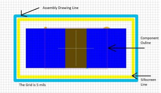
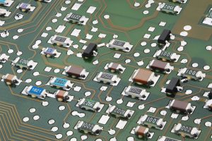
One of the most frequently asked questions of designers who are not yet on board experts is about the division into half. Placing a part too close to another part can create various problems that may require redesign and reconstruction, resulting in a loss of time and money.
Board managers use a few techniques to avoid problems of half and half spaces during integration. They design their trajectory in such a way that there is always enough space between the boundaries of the sections. This minimizes any problems that may arise from getting too close to the parts during installation.
 Example One
Designers should carefully place the parts so that the shape of the bound part does not overlap. For the first example, you can see that placing parts based on a fixed position in place will automatically keep them 50 meters apart. If the board does not have enough space, the PCB Masters can ignore the position bound in place and move the parts closer to each other, remembering the small rules of space division.
Make sure section rules, requirements, and rules of closure are established in your design software. Board technicians have precise space guides for part to half of the different parts. For example, the minimum space between different components such as caps and competitors should always be at least 10 mils, and 30 mils should be optional spaces. This simple act will help to avoid many of the problems of intimacy. These issues can lead to meeting delays or other problems down the line. For more space rules, see Table 1.1.
Table 1.1: Divide Part-to-Part
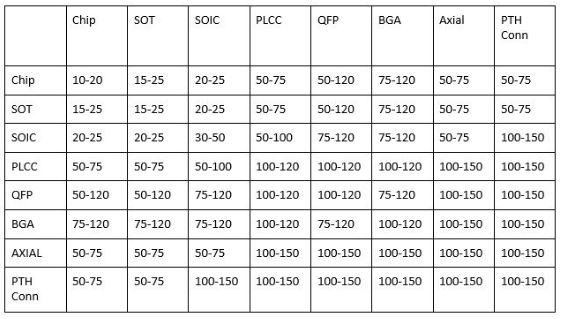
The above values can change, depending on the design constraints and the assembly vendor capabilities.
PCB experts the beginning, the location and size of the parts are no longer a concern and the process of a regional board meeting can proceed without hindrance. This also leads to the next tip.
The board designer should talk to the district designer and engineer to see if part size can be reduced, creating more space on the board. After all, a small portion will mean a little foot on the board.
To learn more about the basics of designing a board read, to know the basics of the basics of PCB design.
Never mix lead-free components with non-specific ingredients to mix without lead. If any component requires lead-free adhesive and no standard lead adhesive is available, then the entire board should be welded without lead and all components should be suitable for welding without lead.
Sometimes the only package available for a particular device is a lead-free BGA. However, boards that will be used for military projects should generally be combined with standard lead solder, according to government requirements. The designer must obtain the customer’s waiver to allow a seamless integration; modify the design to use a pocket-based device to be bonded with a standard lead solder; or have BGA reballed for solder lead (an expensive process that can damage parts).
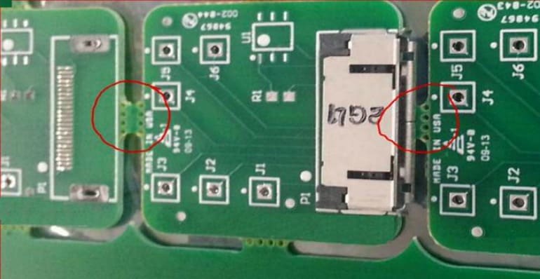
A breakaway tab that remained between these boards after routing interfered with assembling a connector that extends over that edge.
Distribute large sections of the board as evenly as possible during setup, to achieve the best thermal distribution during the solder re-flow. Make sure the convention contractor sews the hot profile of the recessed oven separately for each session.
Whenever possible, avoid mixing technology. The payment for one hole, for example, does not exceed the overtime and the amount spent. It can work best to use more holes or not. If you use through-hole technology, placing all the holes on one side of the board will reduce production time.
Communication between the electrical engineer and the board designer should begin during the initial stages of planning. The designer should review the BOM and carefully inspect the components used in construction. The designer may recommend large parts if there is space on the board and the current design uses smaller parts unnecessarily. This will help to avoid problems during the meeting. For example, it is advantageous to use a capacitor / resistor of size 0402 than 0201 whenever possible.
PCB Master can choose 0805 capacitor over 1206 cap — if 0805 can meet all the required requirements. This will free up valuable space on the board.
Smaller-sized components are more readily available than large components.
They are also built by various vendors. ODB ++ captures the creation, integration, and testing data with an integrated structure that supports automatic analysis and avoids time-consuming data conversion at the CAM stage. Almost all major EDA forums can output design data in ODB ++ format.
Technically, the 10th tip does not look at the design, but part of the contractor delivery. If the assembly is to be done on the basis of the load — some or all of the parts will be given to the customer for the meeting, instead of being purchased by the organizer — the parts should be provided with a carefully designed BOM kit. All parts of the SMT should be provided with rims, or continuous tapes of at least 6 ”lengths, or tubes or trays.
Additional components are required for every part number listed in the BOM list, to cover the termination during the meeting. For example, a composite store may require a minimum of 100 or 20% more 0201 1k ohm resistors than what was called in BOM. Parts of each line item in the BOM should be sent to a clearly marked bag separated from the other parts. All ICs must be shipped in their original, non-invasive protective packaging that includes a desiccant, or they must be baked for eight hours or more to remove moisture before assembly, which may return the assembly day.
In other words, eight strands of eight 1005-size 12-pF capacitors do not meet the BOM requirement of 64 pieces of that segment. The leaflets are too short to load the supply space, and under the best conditions not all parts will end up on the boards. Check and double-check your parts before shipping using our kit guides.
Let me conclude by recommending the best way to avoid assembling problems: Contact your manufacturer before the design begins.
Additional assembly details to keep in mind during the design stage include heating and showering. Make sure you know how high temperatures your parts can be, or can be washed, and the type of mixing you need. If it is to be sold by hand, the design of the board should include the space of the soldering tool.


