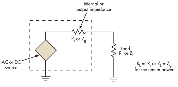
Impedance matching
Impedance matching means that when source is transmitted, the load impedance must be equal to the characteristic impedance of the transmission line. At this situation, the transmission will not reflect, which indicates that all source is absorbed by the load. Conversely, there is source loss during transmission. In HDI PCB design, impedance matching is related to the quality of the signal.
When do PCB traces need impedance matching?
It does not mainly decided by the frequency, but the key is the steepness of the signal, which the rise / fall time of the signal. It is generally considered that if the rise / fall time of the signal (based on 10% to 90%) is less than 6 times the wire delay, it is high speed signal, we must pay attention to impedance matching. The wire delay is generally set to 150ps / inch.
Characteristic impedance
During the propagation of a signal along a transmission line, if there is a consistent signal propagation speed everywhere on the transmission line, and the capacitance per unit length is the same, then the signal always sees a completely consistent instantaneous impedance during the propagation process. Since the impedance remains constant throughout the transmission line, we give the specific name to indicate this characteristic or characteristic of a specific transmission line, which is called the characteristic impedance of the transmission line. The characteristic impedance refers to the instantaneous impedance value when the signal is seen along the transmission line. The characteristic impedance is related to the board layer on which the PCB leads are located, the material (dielectric constant) used by the PCB, the trace width, and the distance between the conductor and the pad, and has nothing to do with the trace length. The characteristic impedance can be calculated using software. In HDI PCB design, the trace impedance of digital signals is generally designed to be 50 ohms, which is an approximate number. Generally, the coaxial cable baseband is 50 ohms, the frequency band is 75 ohms, and the twisted pair (differential) is 100 ohms.
Common methods for impedance matching
Series termination matching
Under the condition that the impedance of the signal source is lower than the characteristic impedance of the transmission line, a resistor R is connected in series between the signal source and the transmission line, so that the output impedance of the source matches the characteristic impedance of the transmission line, and the signal reflected from the load is to suppress a second reflection occurred.
Matching resistance selection principle: The sum of the matching resistance value and the output impedance of the driver is equal to the characteristic impedance of the transmission line. The output impedance of common CMOS and TTL drivers will change with the level of the signal. Therefore, for a TTL or CMOS circuit, it is impossible to have a very correct matching resistor, only a compromise can be considered. Signal networks with a chain topology are not suitable for series termination. All loads must be connected to the end of the transmission line.
Series termination matching is the most commonly used. Its advantages are low power consumption, no additional DC load to the driver, no additional impedance between the signal and ground, and only a resistive element is required.
Common applications: impedance matching for general CMOS and TTL circuits. The USB signal is also sampled this way for impedance matching.
Parallel terminal matching
In the case where the impedance of the signal source is very small, the input impedance of the load end is matched with the characteristic impedance of the transmission line by increasing the parallel resistance to eliminate the reflection at the load end. Implementation forms are divided into two forms of single resistance and double resistance.
Matching resistance selection principle: When the chip's input impedance is very high, for the single resistance type, the parallel resistance value at the load end must be close to or equal to the characteristic impedance of the transmission line; for the dual resistance type, each parallel resistance value It is twice the characteristic impedance of the transmission line.
The advantages of parallel terminal matching are simple and easy, and the obvious disadvantage is that it will bring DC power consumption: the DC power consumption of the single resistance method is closely related to the duty cycle of the signal; the double resistance method no matter whether the signal is high or low Both have DC power dissipation, but the current is half less than the single resistance method.
Common applications: Most applications with high-speed signals.
1.SSTL driver such as DDR, DDR2. It adopts a single resistance form and is connected in parallel to VTT (generally half of IOVDD). The DDR2 data signal's parallel matching resistor is built into the chip.
2.High-speed serial data interface such as TMDS. It adopts single-resistor form, connected in parallel to IOVDD at the receiving device, with a single-ended impedance of 50 ohms (100 ohms between differential pairs).


