Steerable Microwave Beam Phased Array
Steerable Microwave Beam Phased Array
Designer: Levi Sawatzky
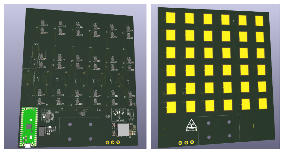
1. Project Overview
This project explores the design and construction of a steerable microwave phased array capable of delivering a tightly focused beam of microwave energy toward a target. This PCB was designed using Kicad and I intend to have it fabricated by PCBway once I secure funding or a sponsorship to bring it within a reasonable budget for a solo hobby project. This project is open source and the Gerber files can be found in the github repository linked as "source code".
1.0. About me
I am a junior electrical engineer from Canada, with a passion for building cool projects that push the boundaries of whats possible. I have a strong interest in electromagnetics, power electronics, and RF / microwave circuits. Some of my past projects include magnetic levetation, tesla coils, plasma generators, and radio transmitters (see them on my portfolio). I chose this project as a way to develop and improve my technical skills in areas that excite me, all while building a cool project that will show flashy, mind-bending results. This project pushes the limits of frequency that can be controlled with electronics. 5.8GHz
1.1. Purpose
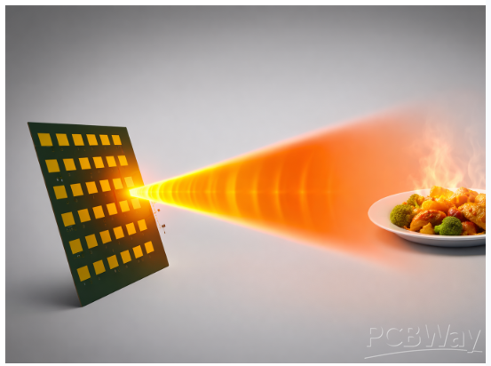
The system serves as a science demonstration platform that reveals the power and elegance of microwave circuit design, phased arrays, and high-frequency PCB engineering. The core concept is to electronically steer a beam of RF energy without any moving mechanical parts, using phase control across an array of patch antennas. This beam can then be used to transfer wireless power across a distance, light up LEDs, heat up food like a microwave, or boost WIFI signal by over 10,000X (dont do this, its very illegal).
1.2. Key Results
A successful project will have the following results:
- Delivers focused microwave energy across a distance
- heats up food, illuminates LEDs across a room
- 50-150 Watts of radiated energy
- Beam forming
- Focuses energy beam as tightly as possible
- ~17° beam waist or 0.5m diameter at 2m
- Implementation of phased-array beamforming
- Steers over a range of 75° in 1 axis
- 4 programmable angles
- Extra things to show off (stretch goals)
- Plasma generation inside noble gases
- Recover radiated energy using a receiver antenna array (wireless drone charger?)
2. System Architecture
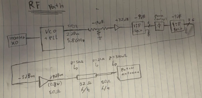
The beam is formed using a phased array of microstrip patch antennas. Each antenna element is driven with controlled phase offsets, allowing constructive interference in a desired direction and destructive interference elsewhere.
Core blocks include:
- RF signal generation
- Power amplification and attenuation
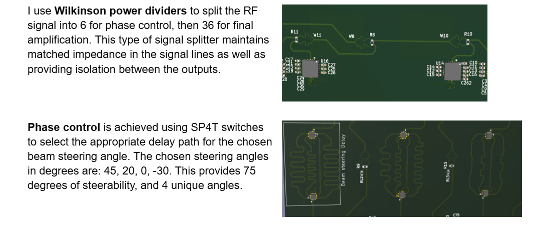
- RF splitting network
- Phase shifting network
- Impedance matching and length tuning
- Patch antenna design & array layout
A simplified sketch of the RF design is shown below.
3. Design Process
The design process involved lots of simulation. I used Ansys HFSS to optimize antenna shape, tuning, and impedance matching. I used python to simulate the array’s beamforming characteristics and beam steering.
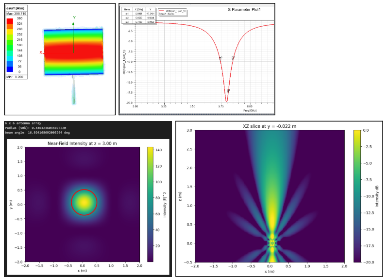
Simulating the antenna shape using Ansys shows a 10dB bandwidth of 10MHz.
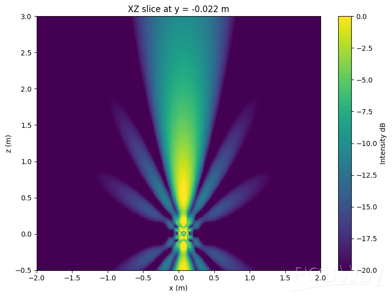
Simulating the beam from my array using python reveals a 3dB beam dispersion of 17 degrees.
4. PCB design
6 layers. 170x200 cm
Impedance controlled
Component count: 398 (34 unique)
PCB cost ~$370
Parts cost: ~$400
Assembly cost: ~$170
4.1 Stackup
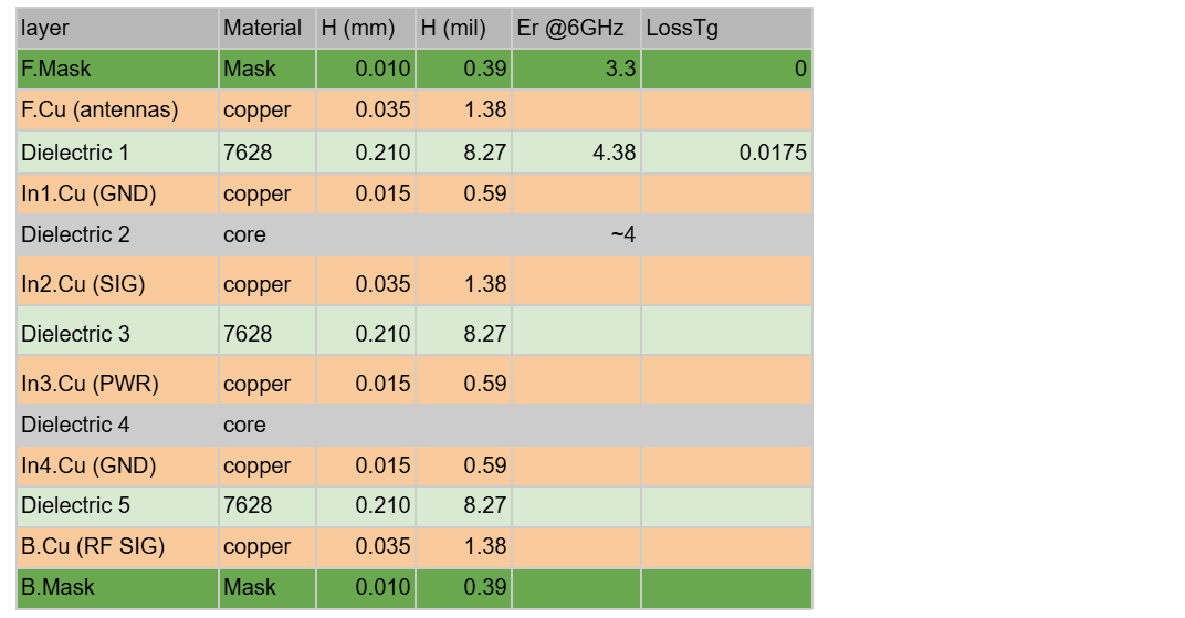
The following stackup was chosen using the 7628 dielectric material because of its affordability, low loss tangent, and its thickness - allowing for wider transmission lines, and less loss for high power signals. This also performed well in antenna simulations - giving the best bandwidth. This stackup was then used to calculate trace width for transmission lines, and propagation delay for the length tuning elements.
4.2 Microstrip Impedance Matching
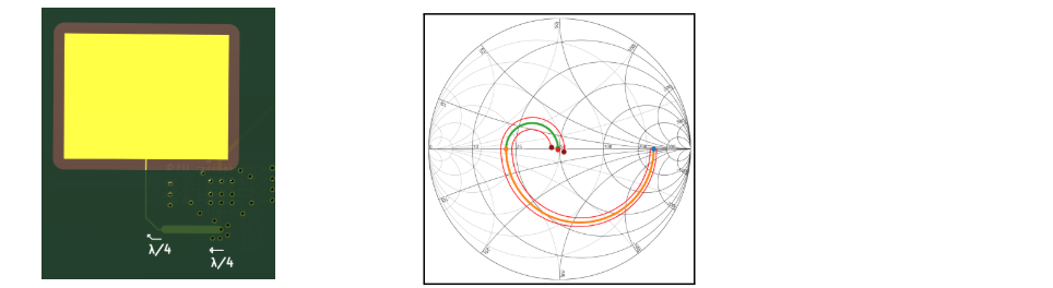
Quarter wavelength transformers are used to match the ~300 ohm patch antennas to the 50 ohm amplifiers. QWT was chosen over stub or lumped element matching due to its robustness: 20% inaccuracies in either the length or line impedance still lands with a manageable 10dB return loss. (this is now unnecessary with the new stackup allowing for antennas being 50 ohm)
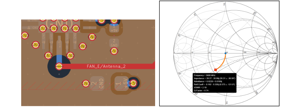
Vias can cause impedance mismatch. The vias in my board are 1.6mm tall from the top to bottom layer. This is about 23 degrees of electrical length. Simulating my original via design (using Sierra via impedance calculator) revealed ~20 ohm vias resulting in a considerable impedance mismatch: increasing the VSWR above 2. Changing the via’s parameters (increasing the antipad size). Allowed me to tune the via impedance to 50 ohm: mitigating the mismatch
4.3. Thermal Considerations
The chosen microwave power amplifiers (SE5023L-R) are designed for telecommunication, and therefore have high linearity implying low efficiency. I estimate that using these amplifiers on a single tone at 1-4W output power, will result in efficiencies of ~25-35%. That means up to 7W of waste heat per amplifier: that’s 36W/cm^2. The DCDC converter produces 200W at 96% efficiency. That means up to 8W of heat generated.
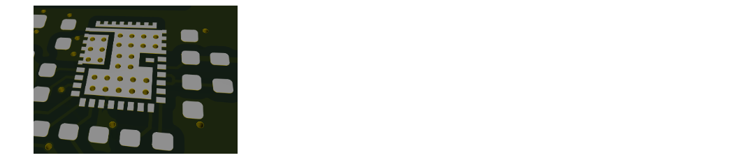
This heat is mitigated through generous via stitching in the thermal pads, and large ground and power planes to spread out the heat quickly. The vias are filled with epoxy to improve thermal dissapation, but temperature will still be the bottleneck of this device's uptime. The device will not be able to operate at max power for extended periods of time, but I hope to achieve bursts of up to 30 seconds.
5. Testing
The biggest risk in this project is the antenna tuning. I need to trust the PCB manufacturer’s material tolerance (dielectric constant, and loss tangent) as well as my accuracy in modeling them in Ansys. (also putting 36 antennas so close to each other likely affects tuning.)
Unfortunately, I do not own a VNA rated for 6GHz, and the cheapest trustable VNA I could buy us upwards of $1100 CAD
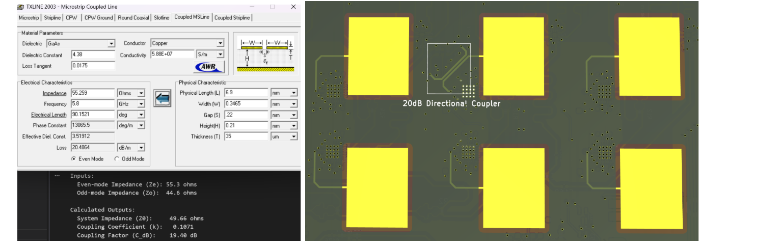
5.1. directional coupler
My solution to verifying antenna tuning is to use a directional coupler between the final stage power amp and the antenna. This microwave circuit can sniff the transmitted and reflected power independently which allows me to calculate VSWR.
6. Technical Challenges
This project was full of technical challenges from start to finish. Many were predicted but many were unexpected.
Sourcing RF components that operate reliably at the target microwave frequency (And which are within my budget)
Managing PCB dielectric tolerances and losses affecting antenna tuning & electrical length
PCB best Thermal considerations under higher power levels
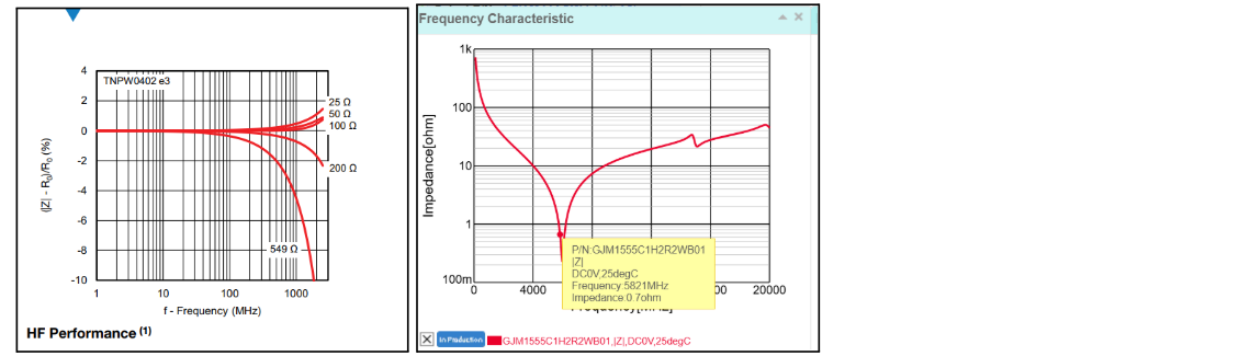
Most resistors and capacitors do not provide documentation of performance at high frequencies - especially as high as 5.8GHz. Below shows impedance vs frequency charts for resistors chosen for the T attenuator, and capacitors chosen for DC blockers. Murata’s “sim surf” website was very handy for choosing appropriate capacitors.
- Comments(0)
- Likes(1)