SIGNALSYNC: A High-Fidelity Analog Signal Splitter PCB
SIGNALSYNC: A High-Fidelity Analog Signal Splitter PCB
Introducing “SIGNALSYNC”: A Precision Analog Signal Distribution Board for Audio, Instrumentation, and Communication Systems:
Welcome to the development of SIGNALSYNC, a custom-designed analog signal splitter PCB engineered for clean, reliable, and low-noise signal distribution. Designed entirely from the ground up using professional PCB CAD tools, this project focuses on maintaining signal integrity while splitting a single analog input into multiple output channels with minimal distortion and interference. The board is optimized for applications involving analog communication, sensor interfacing, laboratory instrumentation, audio routing, RF experimentation, and embedded electronics development. With a carefully organized PCB layout, impedance-conscious routing, and high-quality passive filtering components, SIGNALSYNC provides a robust platform for precision analog signal management.
What Makes SIGNALSYNC Special?
1. Multi-Channel Analog Signal Distribution
SIGNALSYNC is designed to efficiently split incoming analog signals into multiple output channels while preserving waveform quality and minimizing signal degradation. The PCB supports simultaneous signal routing to several output connectors, making it ideal for applications where one analog source must feed multiple subsystems or measurement devices.
This capability is especially useful in:
- Audio signal routing systems
- Sensor signal duplication
- Oscilloscope and measurement setups
- Communication system testing
- Analog instrumentation networks
2. High Signal Integrity PCB Design
One of the key focuses of the project is maintaining clean analog performance throughout the signal path. The PCB layout was carefully designed with:
- Short and optimized trace routing
- Controlled grounding strategy
- Reduced electromagnetic interference (EMI)
- Symmetrical channel organization
- Noise-minimizing component placement
The layout minimizes cross-talk between channels while preserving amplitude consistency across all outputs.
3. Integrated Signal Conditioning Components
The board incorporates high-quality capacitors and supporting passive components positioned strategically near each signal path. These components help:
- Stabilize analog signals
- Reduce unwanted noise and ripple
- Improve transient response
- Enhance overall output consistency
The use of filtering and decoupling techniques ensures cleaner signal transmission even in electrically noisy environments.
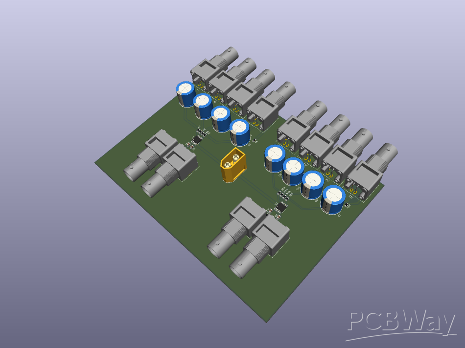
4. Professional Connector Interface
SIGNALSYNC features multiple BNC-style coaxial connectors for secure and reliable analog interfacing. These connectors are widely used in professional laboratory and communication environments due to their:
- Excellent shielding capability
- Reliable locking mechanism
- Low signal loss
- Compatibility with oscilloscopes and RF equipment
This makes the board suitable for both educational experimentation and professional testing applications.
PCB Design and Architecture
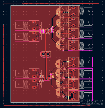
The PCB was designed using a modern electronic CAD workflow, emphasizing both electrical performance and manufacturability.
Key Design Features:
- Dual-channel symmetrical architecture
- Organized analog routing structure
- Wide ground planes for noise suppression
- Carefully spaced traces for isolation
- Compact and modular connector arrangement
- Optimized component placement for balanced performance
The symmetrical layout not only improves aesthetics but also ensures uniform electrical behavior across channels.
Signal Flow and Operation
The operating principle of SIGNALSYNC is straightforward yet highly effective:
- An analog input signal enters through the primary connector interface.
- The signal is routed through conditioning and stabilization stages.
- The PCB distributes the signal evenly across multiple output channels.
- Each output maintains high signal fidelity with minimal attenuation and distortion.
- This architecture enables reliable real-time signal duplication without introducing significant loading effects on the source.
Engineering Focus Areas
- Precision Analog Electronics
- The project emphasizes practical analog electronics principles, including:
- Signal integrity preservation
- Passive filtering techniques
- Ground management
- Noise reduction strategies
- PCB trace optimization
These considerations are essential when working with sensitive analog systems where even small disturbances can significantly impact performance.
Modular Expandability
The modular structure of SIGNALSYNC allows future integration with:
- Operational amplifier stages
- Active buffering circuits
- Differential signal drivers
- RF conditioning modules
- Embedded monitoring systems
This makes the board an excellent platform for continued research and experimentation in analog and mixed-signal electronics.
Applications of SIGNALSYNC
The analog splitter PCB can be applied in a wide range of engineering and research environments, including:
- Audio engineering systems
- Signal monitoring laboratories
- Sensor data acquisition systems
- RF communication experiments
- Embedded systems testing
- Academic electronics research
- Industrial instrumentation interfaces
Its versatility makes it valuable for both educational and professional use.

Our Vision
The SIGNALSYNC project represents a commitment to advancing practical analog electronics design through precision PCB engineering and signal integrity optimization. By combining careful circuit design with professional PCB layout practices, the project demonstrates how reliable analog signal management can be achieved in compact embedded hardware systems.
Through projects like SIGNALSYNC, we aim to deepen our understanding of high-performance electronic system design while developing scalable hardware solutions for future robotics, communication, and instrumentation technologies.
With continued refinement and support from the electronics development community, SIGNALSYNC has the potential to evolve into a versatile platform for advanced analog experimentation and real-world engineering applications.
Apply for sponsorship >>- Comments(0)
- Likes(0)