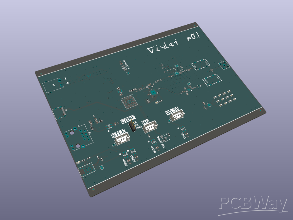
Project Violet: High-Power 6-Layer RF Transceiver R&D
Who I am?
I am a engineering student at SPŠST Panská in Prague, focusing on high-speed digital integration, RF layouts, and advanced embedded systems. Outside the lab, I am an FPV fixed-wing pilot and a competitive sailor (ILCA 6). My obsession with planes, boats, and long-range telemetry is what drives my engineering work:)
Project Violet origin and mission:
Project V.I.O.L.E.T. (Versatile Integrated Optimized - LPI Extreme Transceiver) was born out of operational necessity. After unintentionally retiring my Dragonlink V3 Advanced system and testing ExpressLRS (ELRS) along with MLRS at 868MHz, I realized that modern commercial and open-source systems simply couldn't meet my requirements for ultra-long-range, high-reliability telemetry and controll link. Nothing on the current market trully comes close to the vintage performance benchmarks of legacy systems in this power class.
Instead of compromising, I decided to design a proprietary system to outperform everything available today. Project Violet is a multi-stage hardware research initiative focused on developing a high-performance, long-range (150km+ while in line-of-sight) bidirectional 433MHz data transceiver. This serves as my final graduation design project for SPŠST Panská in Prague, with testing and laboratory validation slated to take place at ČVUT (FEL). If the prototypes succeed, the ultimate goal is to transition this architecture into small-scale commercial production.
Official Filter Partner: Temwell Corporation
A high-power 2W transceiver requires extreme front-end filtering to prevent receiver desensitization and interference to other systems caused by the harmonics. We are incredibly proud to announce that Temwell Corporation has joined Project Violet as our Official Filter Sponsor. Temwell has manufactured and provided a custom batch of high-Q, low-insertion-loss helical bandpass filters specifically tuned for our center frequency. These critical RF components have already completed production ahead of schedule and are currently on-site in Prague, ready for integration into the r0.1 boards once they are made.
The hardware design challenge:
To meet strict signal integrity, high-power RF stability, and strict layout requirements, the transceivers will utilizes a dense, double-sided SMT architecture built on a high-spec 6-layer HDI stackup.
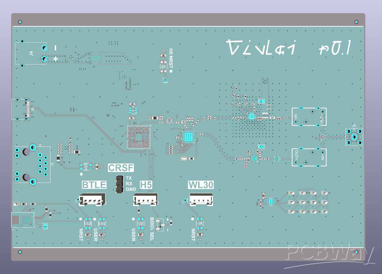
Note: We are currently uploading only the top-side 3D render. The bottom-side render is being updated to cleanly integrate Temwell's official vector logo on the silkscreen and will be published shortly.
*Note on layout geometry: The current r0.1 iteration has been intentionally designed with larger component spacing for better isolation. This will allow us to safely probe, verify, and characterize the core RF architecture without the 2W power amplifier stage blinding or damaging the high-sensitivity LNA front-end. Once the architecture is fully validated, the subsequent r0.2 and r1.0 iterations will move to a highly compressed, high-density layout inside a custom shielded enclosure.
Key technical aspects:
Precision 50Ω Paths: Engineered across 3 areas of the 6-layer stackup with tightly managed coplanar waveguide traces to guarantee maximum power transfer and near zero signal reflection along the 2W transmission line.
High-Speed Silicon Integration: Driven by an advanced STM32H5 MCU (176+25UFBGA package) for low-latency processing, paired with a dedicated Ethernet PHY for robust ground-station data routing.
Solid-State RF Switching: Utilizing the SKY13405-490LF high-linearity switch to handle ultra-fast, low-loss bidirectional RX/TX switching without desensitizing the receiver stage.
True Via-in-Pad (IPC-4761 Type VII): Implementing full resin-filled and copper-capped vias directly within the fine-pitch BGA pads and PA cooling pad. This ensures absolute power integrity and ultra-low inductance decoupling for high-speed stability without risking solder wicking during reflow while at the same time significantly improving thermal stability.
Development Roadmap:
To ensure reliability, the physical layout undergoes a 3-stage iterative hardware development cycle (r0.1, r0.2, and r1.0) over a 9-month window, transitioning from core validation prototypes to fully enclosed field deployment models.
With the front-end filters secured, the r0.1 layout is currently in the final stages of a thorough review. We expect to be production ready in maximum of 2 weeks from the time of writing this article.
Why PCBWay is the Vital Partner for Project V.I.O.L.E.T.
Developing cutting-edge, proprietary RF hardware as entirely self-funded students is an uphill battle. While legacy manufacturers try to lock creators into restrictive, browser-based EDA ecosystems, PCBWay has consistently championed the open-source engineering community by offering native, seamless integration for complex multi-layer KiCad designs.
Beyond software flexibility, Project Violet demands extreme manufacturing precision that hobbyist fabs simply cannot provide. We chose PCBWay because your industrial-grade capabilities - specifically your reliable 6-layer stackups and specialized IPC-4761 Type VII resin via-filling - are exactly what is required to successfully reflow our fine-pitch STM32H5 BGAs and other very fine pitch QFN / LGA components.
By partnering with us, PCBWay isn't just manufacturing a circuit board; you are providing the foundational hardware layer for a system designed to redefine long-range telemetry boundaries. We are incredibly excited about the prospect of featuring the PCBWay logo alongside Temwell on our PCBs, showcasing your precision capabilities to the academic and professional circles at SPŠST Panská and ČVUT (FEL), and partnering with you as we scale from this r0.1 validation prototype toward low-volume commercial production.
Apply for sponsorship >>- Comments(0)
- Likes(0)