Immortalizing Light: Digital Camera System
Hello everyone.
About Me
My name is Jonah, and I’m a rising electrical engineering sophomore at the University of Illinois Urbana-Champaign. I enjoy playing the electric guitar, working out, but most relevant to this project, I am an amateur photographer and aspiring short film maker.
Project Motivation
Since the technology driving photography is image processing algorithms and digital photography, I decided that I wanted to make one myself. I wanted to deepen my understanding within these passions of mine while simultaneously exploring my interests in signal processing, embedded systems, and electronic design. Basically, I think the functionality behind technology is treated as mysterious "black boxes," where to most they’re abstracted to only what they’re used for. As an electrical engineering student, I thought it would be an incredible challenge to build my own from scratch and to uncover what happens “under the hood” of the digital camera. Additionally, being relatively new to engineering (as this is my first major project outside of coursework) I felt there was so much opportunity to learn foundational skills I could apply to future projects and throughout my career; printed circuit boards and embedded systems are everywhere.
Project Description
The camera is going to be powered by an STM32F439 which interfaces to 3 buttons (to control user input), an OV5640 based image sensor camera module, an SD card, and a ST7889 TFT 240x240 display. The three buttons are inputs that affect the current state the camera is in; I have 5 states: idle, view gallery, settings menu browsing, settings menu editing, capturing, and displaying the image.
- Idle continuously updates and pushes new images to the TFT display to serve as a preview for the user when taking photos
- View gallery is to see browse through previous photos taken
- Settings menu browsing is to browse through the settings menu
- The editing state is to edit selected settings
- Capturing is a paused state where user inputs are frozen and an image is captured, processed and written to an SD card, and then frozen to the display
- Displaying the image is where user inputs are unfrozen again and the image is displayed after a capture, allowing the user to use the camera again after the image is processed
In order to receive data and process data from the OV5640, I am interfacing with it via DCMI. With only 256 KB of SRAM there are memory constraints, so I stream the RAW data into row buffers, where the MCU then demosaics the data, applies color space transformations to get the data in the RGB565 format, and gamma is applied from there it streams data to the TFT display. The settings menu comes in here to parametrize this image processing algorithm. Settings, like monochrome, for instance modify the image processing algorithm to performance a luminance calculations at each point and set each RGB value to that calculated value. Gamma for instance changes gamma curve, and in code, it changes the look up table used to gamma encode the image data. When the user decides that want to take a picture, they push one of the 3 buttons and that takes the RGB 565 data and starts encoding the data into jpeg and then it is written to an SD card via the FatFS library.
All of these interfaces will be electrically connected with a circuit board with through hole breakout pin socket connectors to allow for prototyping before the components are completely soldered on by me. Firmware code was written, but DCMI was unable to be setup, due to the MCU on my development board not supporting DCMI. An attempt to parallel read the data and manually poll for signals was made, but ultimately failed due to a race condition forming between the clock of the OV5640 and the storing on data. The MCU was simply not fast enough to store all of the camera data without DCMI. Because of this I’m ordering the breakout PCBs with the STM32F439ZIT6U. I am taking a risk by not ordering a STM32F439ZI dev board and going straight to purchasing PCBs, but I designed the PCBs so that I could prototype with SWD and temporarily pin sockets could be de-soldered and actual modules soldered on later.
Progress Display
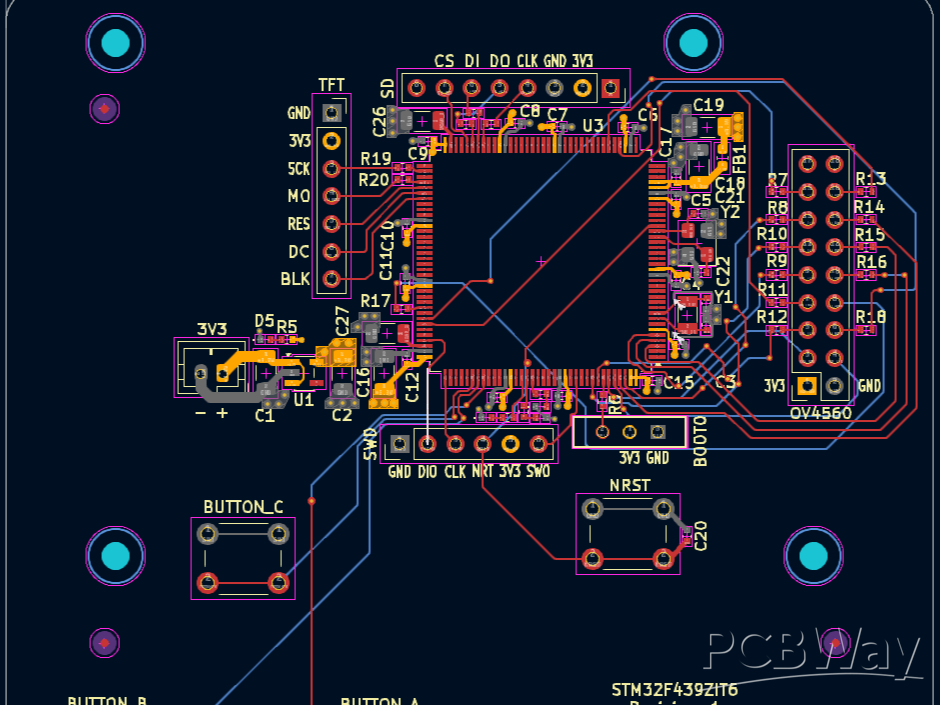
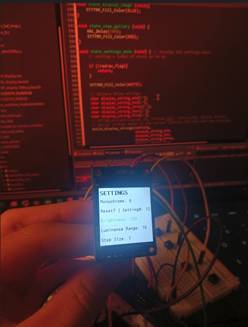
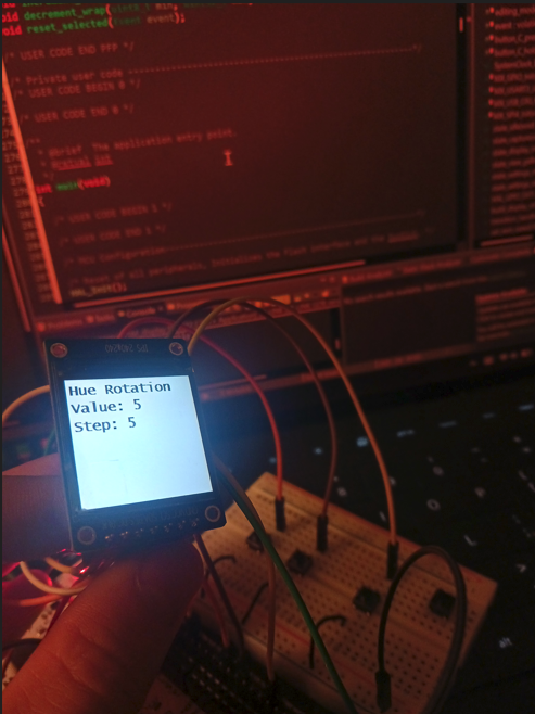
For current progress I currently have kicad schematics and layout completed; the first revision of my PCB is done. On the firmware side I have completed the state machine including the settings menu and editing. I also have interfacing with the display drivers via a library setup, and I have written SD card drivers to write a sample text file.
PCB 3D viewer: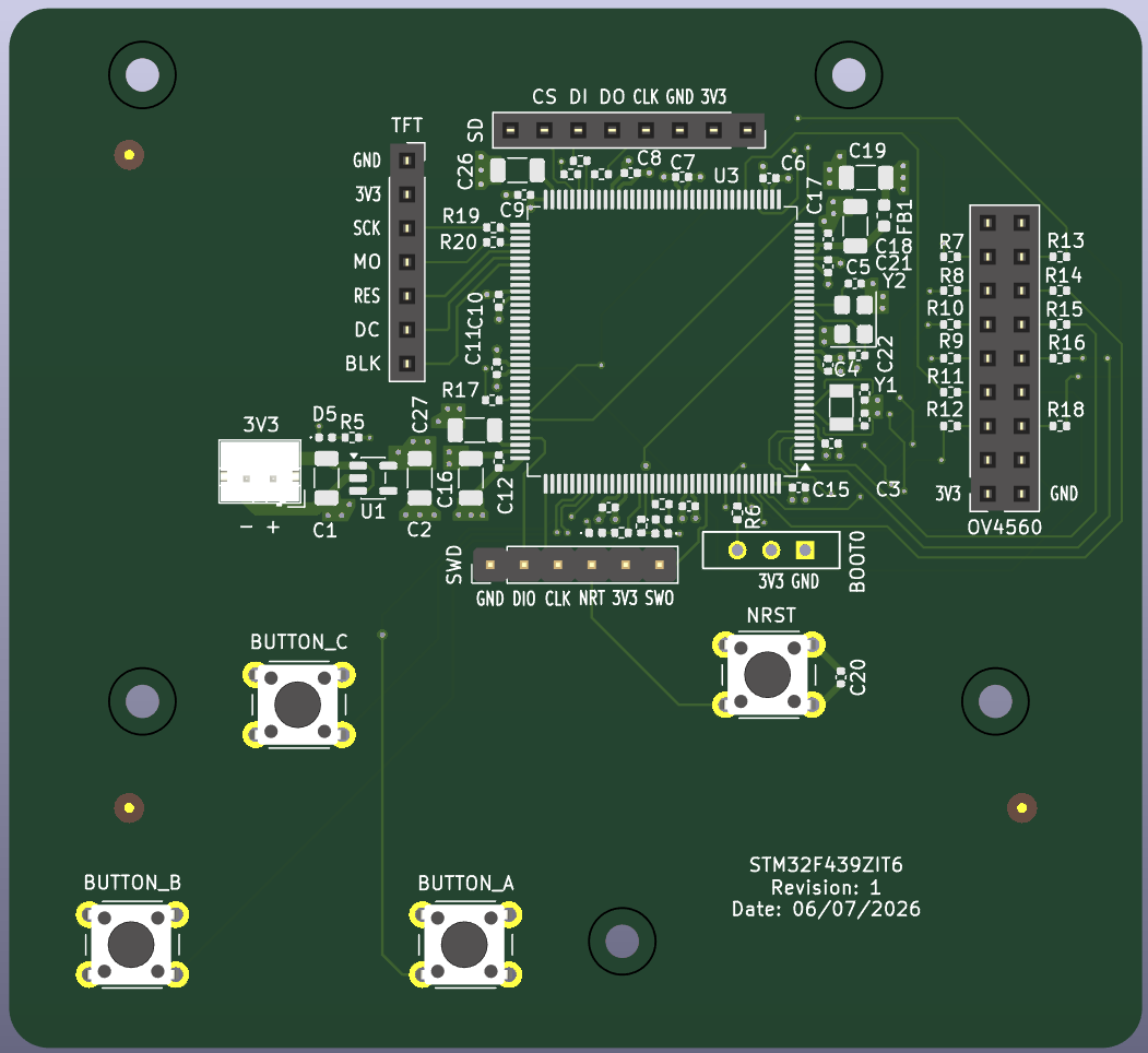
Settings Menu View:
Why PCBWay
As I learning the design process behind PCB’s for this project, I stumbled upon an STM32 hardware tutorial by Phil’s Lab; this video was perfect for me, as I was also planning to use an STM32. In this video, he was sponsored by PCBWay. This video showcased the capabilities of PCBWay very well, as they were able to make the board he designed in the video, meeting all of the requirements. Given that I’m also making a 4 layer stm32 based board with some sensitive signals, I figured PCBWay was more than capable of manufacturing this board.
On top of this, the affordability of PCBWay with the student sponsorship program had me sold on choosing PCBWay. I plan to order 5 PCBs, as this will be the most cost effective for me, I will have multiple PCBs to prototype with and experiment adding other features on. This isn’t cheap however; I still am a university student with budget constraints. That’s why I believe PCBWay’s student sponsorship program can help me immensely. Not only would I benefit, but I would be able to recommend PCBWay as a reliable manufacturer to other students and engineers both in person and online. I believe that my vision deserves to be realized, and my project deserved to be completed.
Apply for sponsorship >>- Comments(0)
- Likes(0)