SMD (Solder Mask Defined) and NSMD (Non-Solder Mask Defined) refer to the way copper pads on a printed circuit board (PCB) are exposed. This seemingly minor detail in PCB pad design, which used to go unnoticed in the past, has become increasingly important in today's trend of shrinking electronic components and smaller solder joints.
What are SMD and NSMD?
At present, both pads and traces are primarily made using copper foil. However, we don't expose all the copper foil when designing PCBs but only expose the pads that need to be connected or soldered to prevent potential issues such as moisture-related short circuits in the future. At this point, we typically use a material known as Soldermask to cover the copper foil that should not be exposed. Therefore, the precision and capability of soldermask printing become crucial, especially for small solder pads.
SMD
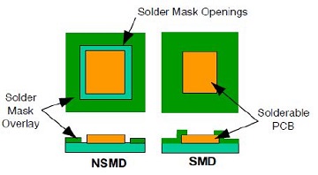
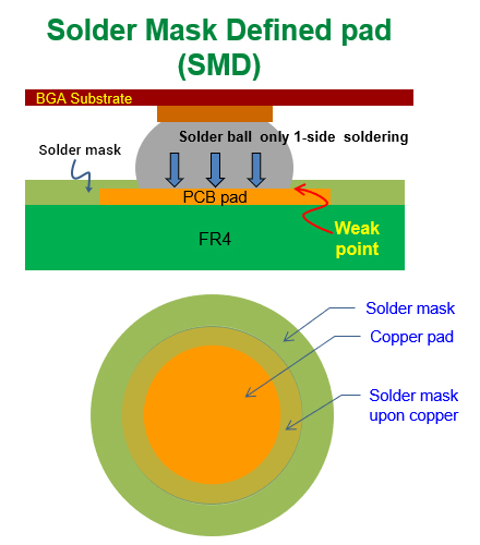
SMD (Solder-Mask Defined) uses soldermask to cover a larger area of copper foil, and the copper foil is exposed where the soldermask does not cover it, which is the pad. The size of this solder pad will depend on the size of the green oil opening, so it is called Solder-Mask Defined Pad.
NSMD
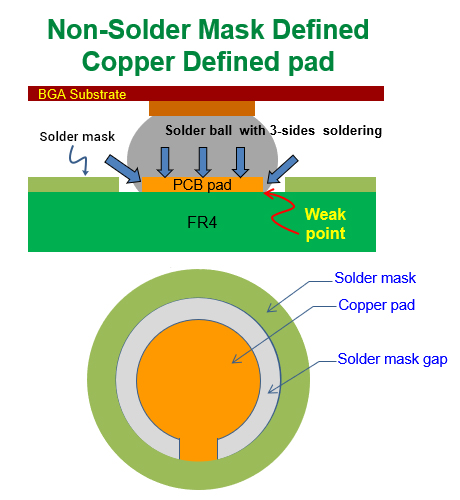
NSMD (Non-Solder Mask Defined), also known as Copper Defined Pad Design, is a design approach where the copper foil is designed to be smaller than the soldermask opening, somewhat resembling an island in a lake. In this design, the size of the solder pad is primarily determined by the dimensions of the copper foil, hence it is referred to as Copper Defined Pad Design, or alternatively, a Non-Solder Mask Defined.
Advantages and Disadvantages of SMD and NSMD
Advantages of SMD
- SMD solder pad shapes are regular and not affected by trace routing, making them suitable for small component pads such as 0402, 0201, and 01005.
- SMD solder pads are less prone to tearing and detachment during rework because the actual copper foil size of SMD pads is relatively larger compared to NSMD, and a portion of the pad is covered by soldermask, which results in a stronger bond between the solder pad and the FR4 substrate.
Disadvantages of SMD
- SMD, due to the solder mask covering the solder pad, results in a stencil thickness that is one soldermask thickness higher than NSMD, increasing the solder volume and making it more prone to short circuits during the manufacturing process. Special attention is needed in this regard.
- It reduces the available copper surface area for solder connections and decreases the space between adjacent solder pads. This limitation affects the trace widths between the solder pads and may impact the use of through-holes, making PCB layout more challenging.
- The solder strength of SMD solder pads tends to be relatively weaker. This is because the effective solderable area is reduced due to the smaller size of the SMD pad, and the presence of soldermask around the SMD pad can lead to thermal expansion and contraction during reflow soldering, affecting the solder wetting at the border between solder and soldermask.
Advantages of NSMD
- Because NSMD solder pads consist of independent copper foil, during soldering, not only the top surface of the copper foil wets with solder but also the vertical sides around the copper foil can be wetted. Consequently, NSMD pads have a relatively larger solderable area, leading to better solder joint strength.
- There is greater spacing between solder pads (compared to SMD), allowing for wider trace widths and more flexibility with the use of through-holes, which makes PCB layout easier.
Disadvantages of NSMD
- The shape of NSMD solder pads is influenced by trace routing and may result in varying pad sizes on the same chip. The "tombstone" effect can be observed. It's recommended to use SMD pad designs for flex boards and small devices (those smaller than 0402) while using NSMD for larger components, as NSMD designs are relatively simpler. For BGAs, a mixed approach can be employed, with functional pins using SMD design and fixed pins using NSMD design.
- NSMD pads are isolated, making them relatively more prone to detachment during repair or rework.
- Flux residue and solder balls can easily accumulate in areas not covered by soldermask.


