By Hesam Moshiri, Anson Bao
A DC-to-DC converter is one of the most commonly used circuit topologies in electronics, especially in power supply applications. There are three major types of DC-to-DC converters (non-isolated): Buck, Boost, and Buck-Boost. Sometimes a buck converter is also called a step-down converter and a boost converter is also called a step-up converter.
In this article/video, I introduce an adjustable buck converter circuit that uses an advanced converter chip, made by Texas Instruments, which is TPS5430. It’s a high-frequency and 95% efficient chip. In the PCB layout design of such converters, several PCB design rules should be followed, otherwise, the circuit might generate a significant amount of radiated emission and suffer output instability.
To design the schematic and PCB, I used Altium Designer 22 and used the manufacturer part search feature to directly import the components into the PCB project. Then, generated the BOM list using the free OctoPart services. To get high-quality fabricated boards, I sent the Gerbers to PCBWay and tested the circuit for output stability and noise, using a DC load, A multimeter, and an oscilloscope. Soon later, I will also perform the step-response test and demonstrate the results. Stay connected!
Specifications
Input Voltage: 5.5V to 36V
Output Voltage: 1.22Vmin (variable)
Output Current (continuous): 3A
Output Current (peak): 4A
Maximum output voltage drop: 10mV (3A load)
Output Noise: 12mVp-p (no load), 43mVp-p (3A load), 20MHz-BW
Download the Gerber or order 10Pcs high-quality boards, for just 5USD
To order a fully assembled PCB board (Plus FREE shipping). Please contact: anson@pcbway.com
Circuit Analysis
Figure 1 shows the schematic diagram of the device. As it is clear, the heart of the circuit is IC1 (TPS5430).
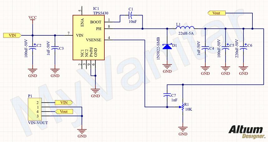
Figure 1
Schematic diagram of the 36V-3A Adjustable Efficient DC to DC Step-Down Converter
P1 is a 4-pins male pin header that provides input/output connection to the board. C2 and C3 are input capacitors that are used to reduce the input noise.
IC1 is the TPS5430 [1] buck converter chip that is an efficient and advanced chip made by TI. According to the datasheet: “converter that integrates a low-resistance high side N-channel MOSFET. Included on the substrate with The TPS5430-Q1 is a high output current PWM the listed features are a high-performance voltage error amplifier that provides tight voltage regulation accuracy under transient conditions, and an Undervoltage lockout (UVLO) circuit to prevent start-up until the input voltage reaches 5.5 V, an internally set slow-start circuit to limit inrush currents, and a voltage feed-forward circuit to improve the transient response. Using the enable (ENA) pin, the shutdown supply current is reduced to 18μA typically. Other features include an active-high enable, overcurrent limiting, overvoltage protection (OVP), and thermal shutdown. To reduce design complexity and external component count, the TPS5430-Q1 feedback loop is internally compensated. The TPS5430-Q1 regulates a wide variety of power sources including 24-V buses.”
PH is the output pin of the chip. Therefore, D1 [2], L1, C4, C5, and C6 are typical buck converter elements. R1 adjusts the output voltage and C7 was used to reduce the noise.
PCB Layout
Figure 2 shows the PCB layout of the design. It’s a two layers PCB board and all components are SMD. There are a PCB few design rules that should be followed in designing such circuits. Please watch the video completely.
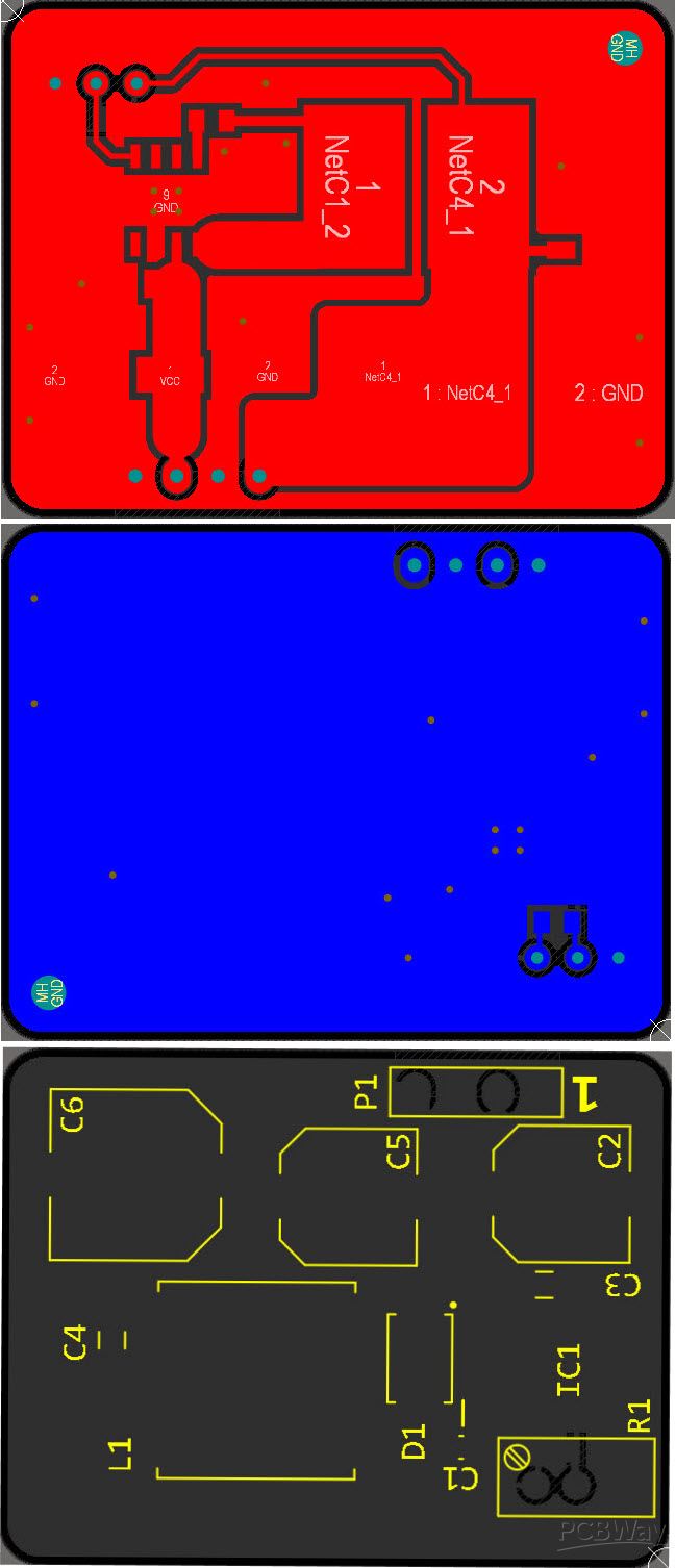
Figure 2
PCB layout of the adjustable DC to DC buck converter circuit
When I decided to design the schematic and PCB for this project, I realized that I don’t have the component libraries of IC1 and D1 in my component libraries storage. So, I used the Altium Designer’s “Manufacturer Part Search” feature and quickly imported and installed all missing components (Figure 3).
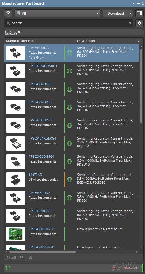
Figure 3
Altium Designer Manufacturer Part Search (the selected component is TPS5430)
Figure 4 shows a 3D view of the PCB board and assembly drawings.
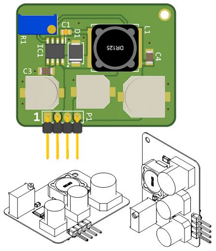
Figure 4
A 3D view of the PCB board and assembly drawings
Test and Verification
There are 3 tests to examine the performance of a buck converter: Line/Load regulation, output noise, and step-response test. Please watch the video for more details. The converter board demonstrated around a 10mV voltage drop only, under a 3A load. Figure 5 shows the output noise with no load at the output and figure 6 shows the output noise by applying a 3A load (using a DC load). This noise can be easily reduced even further by adding some decoupling capacitors just as close as possible to the load.

Figure 5
Output noise of the buck converter (no load)

Figure 6
Output noise of the buck converter (3A load)
Bill of Materials
I used the OctoPart website to generate the bill of materials (figure 7). It is free, easy, and fast.
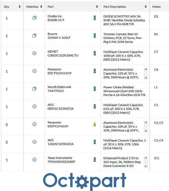
Figure 7
Bill of materials of the DC-to-DC buck converter
References
[1]: TPS5430: https://octopart.com/tps5430mddarep-texas+instruments-12192395?r=sp
[2]: B360B-13-F (or SS34, SMB package): https://octopart.com/b360b-13-f-diodes+inc.-325834?r=sp


