Summary: Here, we will learn how to design a simple PCB.
In this post, I'll be showing you guys how we can design your own PCBs for our projects. Everything in this post is free. All you need to get started with your first PCB layout is just a web browser.
The first thing you need to do is go to Altium’s website and you can create a free account. The advantage of having a free account is you can draw the circuit, create a layout and save it online. Once you save it you can access it from literally anywhere. All you need is a web browser. You can even collaborate or share your design with your friends as well as your clients.
This is an account I just started. To get started click on this create button and create the project. Here you can give your project a name. I'll be naming it as "LED demo". Now scroll down to the bottom and click "save and open in editor".
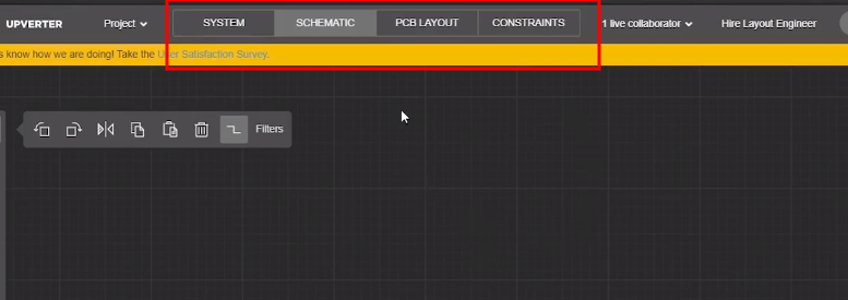
Now that will open up a canvas where you can start your work.
This is where we'll be drawing our circuit. Now if you take a closer look, you will be able to see some tabs over the canvas. Schematics, PCB layout, etc.
We will be drawing the circuit in the schematics tab and once we are done with the circuit we will be using this "PCB layout" tab to design our PCB. Now we will go to the schematics tab and start adding components.
You see this button here.
This is the 'components' button. You can click on that and add your components. Here you will find almost all the components you will need for your projects.
In the search box, type LED and hit enter then it will list out all the different types of LEDs you can use for your project. Here one thing to keep in mind if you are planning to design a PCB layout is, the component you are going to use does have a proper footprint. Only then it will show the component under the PCB layout tab. If you want to get more information about any components in this list, just click on this button and it will show you the footprint of that component.
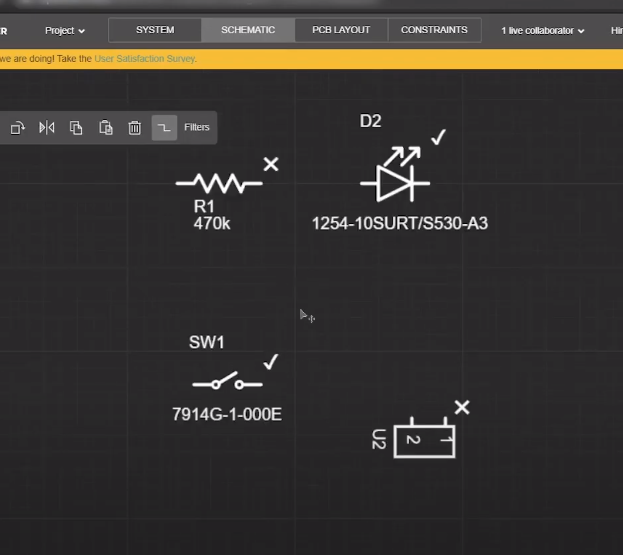
For now, we'll be using this LED. Now close that window and you can place that component to the schematics. Lets finish by adding the remaining components.
We have now added all the components. We have the header, switch, resistor, and LED. You should also see all these components under the PCB layout tab.
Now, we will finish the circuit by connecting all the components and drawing the circuit. To connect all the components, you can use this net tool.
Using this net tool you will be able to connect all the terminals of the components the way you want. So here we connect the positive terminal of the battery to the switch, switch to the resistor, resistor to the LED, and LED to the negative terminal of the battery.
So the schematics are now ready. Now we will take a look at the PCB layout. Go to the PCB layout tab and you will see connections in all the components.
But these connections are logical connections and there are no physical connections. To make a physical connection we will need to draw the tracks that connect all the components before drawing the tracks you have to arrange the components properly.
You have to place and align the component in such a way that it will be easy for us to route and there won't be any wastage of space.
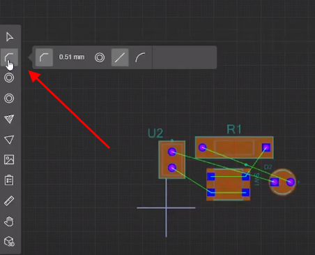
To route the components, you can use this trace tool.
So select the trace tool, zoom in, so that you are comfortable with the view, and start connecting all the terminals of the components. Actually it's very easy to draw the tracks, but if you make a small mistake here, it will change the entire circuit and you won't be able to use this PCB for that purpose. So you have to carefully connect the footprints of all the components.
Another thing to notice is that the dark blue tracks we are drawing are actually on the top side of the board.
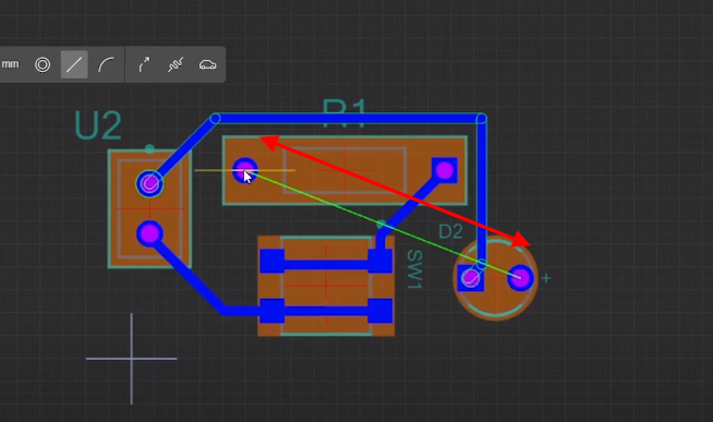
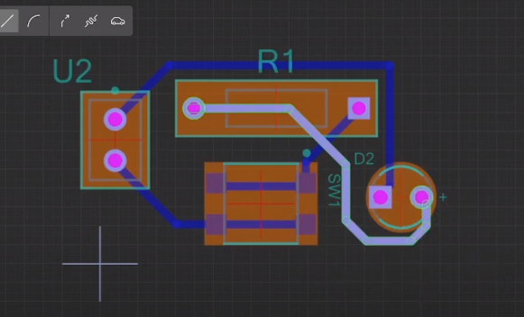
We have almost completed the circuit but one connection is still remaining.
We have to connect the resistor to the LED, but here is a problem. Whichever way we try to connect, the new track will always intersect with any of these previous tracks. So what we are going to do is, we are going to draw that track on the bottom side of the board.
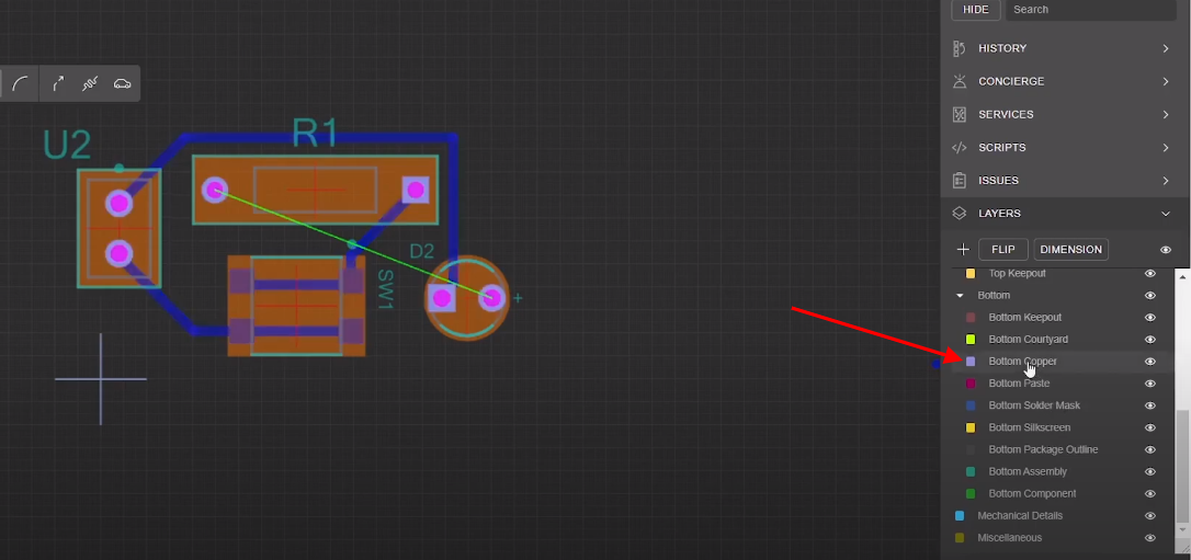
To select the bottom layer, go to layers > bottom and select the bottom copper layer.
Now we can continue with the circuit. These light blue tracks are actually on the bottom side of the board. The dark blue on the other hand is on the top side.
That means even if the dark blue and the light blue lines intersect in this canvas, that won't be a problem in the physical board because both these lines are on either side of the board.
Now all the components are connected using tracks it's time for us to draw the boundary for the board. Each board will be cut on that shape.
The advantage of the Altium Upverter is that you will be able to draw different shapes very easily.
To draw a boundary for your board, click on this path tool. Here I'll be drawing a simple outline for this board. So before you start drawing, you have to select the right layer.
Go to layers and select mechanical details. Now, you can select the path tool and draw a simple outline around the circuit. You can draw so many complex outlines for your board within seconds.
That's it. So once you are done drawing with the tool, you can press escape. Our PCB layout is now ready. Now you can export this PCB file in whichever format you want. There are so many supported file types to export this PCB file.
Go to projects > export files > and select the format you want.
Here I'll be downloading the Gerber file. So we have the Gerber file now. So this was easy right. Now all you have to do is order it online.