A thermal relief pad is a technique used in PCB design to reduce thermal stress problems. It includes copper spokes that extend from the pad to the surrounding copper plane.
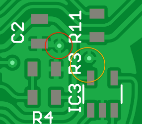
Figure 1: Thermal relief pads
Thermal relief pad functions
Firstly, thermal relief pads are used to address uneven heat distribution during the soldering process. Copper pours are large areas of copper on a printed circuit board that are not part of a trace or component pad. When large copper pours are present, they can act as heat sinks and absorb heat from the soldering iron, making it more difficult for heat to reach the component pad and create a strong solder joint. This can result in soldering defects such as tombstoning, cold solder joints, and solder bridging. Thermal relief pads are designed to mitigate these issues by creating a small gap between the copper trace and component pin, allowing heat to be more effectively directed to the component pad and ensuring a reliable connection.
In addition to improving heat distribution during soldering, thermal relief pads also help prevent overheating and component damage. Directly connecting a component pad to a copper pour can impede heat flow and cause the component to overheat and potentially fail. By using a thermal relief pad, heat can be more easily conducted away from the pad and into the surrounding copper areas, improving heat dissipation and preventing overheating.
Whether or not to incorporate thermal relief pads into a PCB depends on the specific requirements and constraints of the design. For example, if the design does not involve high-power components or large copper pours, or if the assembly process does not involve wave soldering, then thermal relief pads may not be necessary.
Thermal relief pad design consideration
Here are some design considerations for thermal relief pads.
Through-hole components typically have larger pins that require more heat during soldering. Thermal relief pads are commonly used in through-hole components to ensure proper heat dissipation. When designing thermal relief pads for through-hole components, it's important to determine the appropriate size and shape of the pad based on the component size and lead diameter. A larger pad will typically require more spokes to ensure proper heat dissipation. The trace width, layer thickness, and copper weight are also factors that can affect the size and shape of the thermal relief pad.
For surface mount components, thermal relief pads are typically used in the form of in-via pads. The via functions as the thermal relief device, allowing for proper heat dissipation while also maintaining clearance around the edge of the pad. It's important to ensure that the via is properly sized and located to provide adequate heat dissipation. The orientation of the pad is also an important consideration, as it can affect the amount of heat that is transferred to the component during the soldering process.


