PCBWay Community
Search title or content
Search
PCBWay
PCB Instant Quote
CNC | 3D Printing
Login
Sign Up
More Notifications
No notifications.
My Profile
My projects
My Likes
My Deals
My Goods for Bazaar
Settings
Sign Out
Projects
Categories
DIY Electronics
Arduino
Hardware
Audio
Computers & USB
Breakout Board Projects
Home Automation
LED Displays & Matrices
IoT
Robotics
View all categories
By Source Files
Onju Voice - AI assistant replacement to Google Nest Mini by @justLV
LogicAnalyzer V6.0
DIY 1kW Open Source MPPT Solar Charge Controller
Tad Boy Color
SummerCart64 - a fully open source N64 flashcart
kv4p HT v1.7b
QuinLED-Dig-Uno
Bike Fingerprint - PCB
Arduino RC engine sound & light controller with inertia simulation for ESP32
Solar Powered WiFi Weather Station V2.0
Frog Boy Color
SIDKick pico 0.2 (SID 6581/8580-replacement for C64/C128)
View all source files projects
Featured Projects
Onju Voice - AI assistant replacement to Google Nest Mini by @justLV
LogicAnalyzer V6.0
DIY 1kW Open Source MPPT Solar Charge Controller
Featured
Source Files
Video
View all projects
Questions
Sponsorships
Feedback
Blog
Store
PCB Design
Contest
- 2026 KiCad PCB Design Contest
- 8th Project Design Contest
- 7th Project Design Contest
- KiCad Design Contest
- 6th Project Design Contest
- 5th PCB Design Contest
- 4th PCB Design Contest
- Raspberry Pi Pico Contest
- PCB Design Tutorial
- 3rd PCB Design Contest
- I CAN SOLDER Kit Contest
- 2nd PCB Design Contest
- 1st PCB Design Contest
Add questions
Create a project
Please verify your email address so that you can enjoy our more comprehensive services.
Wearables
Weather
All categories
DIY Electronics
Arduino
Hardware
Audio
Computers & USB
Breakout Board Projects
Home Automation
LED Displays & Matrices
IoT
Robotics
3D Printing
Blinkenlights
Calculator
Camera
Clocks
CNC
Educational
Automotive
Electronic Games
ESP32
Fabrication Tools
Flight
Guitar
Keyboards
Misc
Music
Nixie Tube
Oscilloscope
Particle
Power Supply
Programmable Logic Projects
Raspberry Pi
Radio
Retro Stuffs
Space & Satellite
Sensors
Software
Synthesizer
Ultrasonic
Virtual Reality
Wearables
Weather
Project by top creative fields
All categories
3D Printing
Arduino
Audio
Automotive
Blinkenlights
Breakout Board Projects
Calculator
Camera
Clocks
CNC
Computers & USB
DIY Electronics
Educational
Electronic Games
ESP32
Fabrication Tools
Flight
Guitar
Hardware
Home Automation
IoT
Keyboards
LED Displays & Matrices
Misc
Music
Nixie Tube
Oscilloscope
Particle
Power Supply
Programmable Logic Projects
Radio
Raspberry Pi
Retro Stuffs
Robotics
Sensors
Software
Space & Satellite
Synthesizer
Ultrasonic
Virtual Reality
Wearables
Weather
View all categories
Radio
All about radio with PCB.
All tags
Radio
SDR
VFO
SSB RADIO
FM
Create a project
Sort by : Trending
Trending
Score
Likes
Views
Discuss
Newest
Featured
Source Files
3D Design
Video
UPDATE Jan 25, 2025:This design is now obsolete. Please use v1.8 instead which has far better transmit power and receive sensitivity, and fits more ESP32 dev boards! Find it here:kv4p HT v1.8a (1" wid...
kv4p HT v1.7b
33348
32
48
Vance Vagell
Vance Vagell
UNITED STATES OF AMERICA
52
0
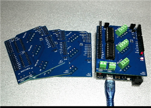
This shield was designed with no particular project in mind. It aims to be useful for both automatic and keypad-operated antenna selectors in general. This is just hardware, providing slightly more th...
Antenna (or whatever) Selector SHIELD for Arduino Uno
135
1
1
Mire YU2ZZ
Mire YU2ZZ
SERBIA, REPUBLIC OF
0
2
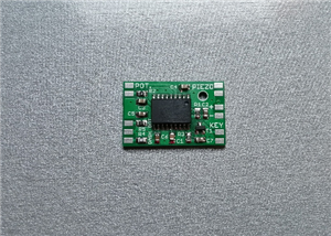
This is a Morse keyer by DL4YHF, who designed the circuit and wrote the software 26 years ago. I just designed a new PCB for it. The circuit is practically the same, with only a few minor changes and ...
‘PIC-Keyer’: 2025 Edition
91
3
1
Mire YU2ZZ
Mire YU2ZZ
SERBIA, REPUBLIC OF
0
2
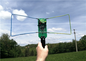
A diode will conduct RF only if it is forward-biased; that is why it can be used as a DC-controlled RF switch. The 4047 integrated circuit operates as an oscillator that alternately turns on two switc...
Simple but Smart Radio Direction Finding for VHF and UHF ‘Fox Hunting’
93
1
0
Mire YU2ZZ
Mire YU2ZZ
SERBIA, REPUBLIC OF
0
2
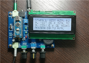
This real-time Morse decoder and trainer uses the Goertzel algorithm to detect a CW tone of 708 Hz. The program then analyzes the detected tone patterns in order to recognize and decode Morse characte...
Arduino-Based DSP Morse Decoder and Trainer
109
3
0
Mire YU2ZZ
Mire YU2ZZ
SERBIA, REPUBLIC OF
0
2
The interface has been successfully tested with Win-Test and DXLog under Windows 10 and Windows 7 (both 32-bit and 64-bit), and with N1MM under Windows 10. It should also work with any other logging p...
USB CW Keying Interface
96
3
1
Mire YU2ZZ
Mire YU2ZZ
SERBIA, REPUBLIC OF
0
2
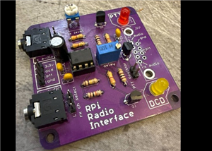
Selectable transmit and receive channelsI noticed between sound card dongles, the mic input could be on the left or the right channel, depending on how much care the manufacturer put into it. A jumper...
RPi-WD-Packet-Interface - A digital mode soundcard interface for the Raspberry Pi!
37
0
0
Ham Radio Lurker
Ham Radio Lurker
ARGENTINA
0
0
Radio Controlled/Wireless Coconut harvester is a very helpful machine to harvest a lot of coconut fruit without risking the health or lives of any harvester by climbing the coconut tree and harvest t...
Wireless Coconut Harvester Machine || Coco-bot Harvester Arduino Nrf24l01 based
20622
16
39
AA ELECTROTECH
AA ELECTROTECH
PHILIPPINES, THE
33
1
CASSIOPEIAThe ultimate (2021 at list) model rocket launchpad 3 min. readingCassiopeia is the launchpad electronic for Athena and hopefully for other rockets too. We hope it will be a timeles...
Cassiopeia Rocket Smart Launchpad
6879
10
9
Christian Ferracane
Christian Ferracane
ITALY
22
0
Automatic matching devices are very rarely found in homemade radio amateur designs. As a rule, radio amateurs use homemade external hand tuners or purchased automatic ones. The proposed device, develo...
Automatic Antenna Tuner 5x5 ATU-100 mini by N7DDC
26491
0
21
Alexiev
Alexiev
BULGARIA
149
0
uSDX – An Arduino based, DIY, QRP, SDR, All mode HF Transceiver – PCB Iteration V1.02uSDX is an Arduino based SDR all mode HF QRP transceiver project brain child of Guido PE1NNZ.BARBAROS A?URO?LU took...
uSDX – An Arduino Based SDR All Mode HF Transceiver
37717
7
32
Alexiev
Alexiev
BULGARIA
149
0
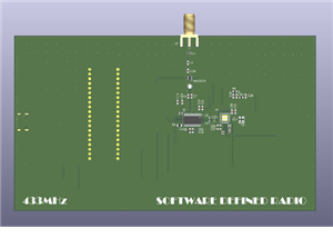
SOFTWARE DEFINED RADIO The designed printed circuit board is a doubled sided 4-layer stacked 433MHz Software Defined Radio module that takes in radio signals and converts into equivalent baseband...
Software Defined Radio
351
3
3
Kushaal Veeraraghav
Kushaal Veeraraghav
INDIA
0
0
OverviewThe 8-channel RC transmitter and receiver system crafted for the PCBWay 6th Contest is a highly intricate and technologically advanced solution tailored for remote-controlled applications. By ...
Advanced 8-Channel RC Transmitter and Receiver using stm32f103c8t6,nrf2l01.(Totally Diy)
3782
4
7
DIY TECHOS MR AHSAN BILAL
DIY TECHOS MR AHSAN BILAL
PAKISTAN
59
0
wireless controlerd ipod made because i keeped loseing the remote so i made it completly wireless with the help of a pi pico how it works:the pi pico will wait for a bluetooth command to be sent and a...
bluetooth ipod classic dock
4063
0
2
yuno
yuno
UNITED KINGDOM
0
0
Robotic system controlled by an embedded microcontroller with Bluetooth communication for remote operation with a Smart Phone with ANDROID Operating System from where it can not only be directed so al...
Sniffer Robot Explosives Detector
3185
0
5
MiguelCGL
MiguelCGL
COLOMBIA
1
0
Since my first robotic project I use game controllers to execute commands and functions. This is certainly an influence of my gamer days. I already did projects with PS2, Xbox 360 controllers... but t...
N64-inspired robot controller (Arduino + nRF24L01)
4702
5
5
Mech-Dickel Robotics
Mech-Dickel Robotics
25
0
1
2
3
4
5
6
7
8
9
10
11
...