Summary: In this PCB Design Tutorial, I have explained all the major steps to design a PCB with Diptrace. I have covered how to draw schematics, routing the board, generating Gerber files for manufacturing the PCB. And I have used all the FREE resources to design the PCB.
Before designing the PCB, you have to draw the schematic. So, I have explained all the steps of drawing schematic in DipTrace.
First, Go to "File / Titles and Sheet Setup" from the main menu, then select ANSI A from the Sheet Template drop-down box

After that go to the bottom of the dialog and check the Display Titles and Display Sheet items. Then press OK.

To enter text in the title field, hover over that field with the mouse, then left-click on it to open the field properties pop-up dialog box, then type in the text (field content), define alignment (Left, Right, or Center), and the font.
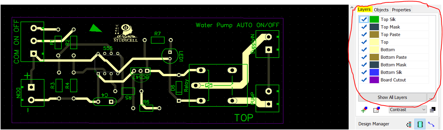
In DipTrace, libraries are organized into standard and custom library groups with multi-level search filters, which helps to find the correct components quickly. The Component panel has all the required tools to place components and manage libraries.
First, you have to drag and drop all the required components. Let's start with 555 Timer IC.

To find any components, you can turn on the filter, then search for the component. Here I have searched for 555 Timer IC.
Now to place the component, click on the component in the list (Left side) and move your mouse pointer to the design area. Then Left-click once to place one selected component. After that, Right-click to disable the component placement mode.

In a similar way search for all the required components, and place those components in the design area.

Now, Connect pin-5 of 555 IC to pin-1 of the capacitor C4. You need to make sure that you are in the default mode. Hover with the mouse arrow over pin-5 (CVOLT) of 555 IC, and left-click it - the Place Wire mode will be activated automatically. Then move the mouse arrow down to the pin-1 of the C4 capacitor, and left-click it to connect the wire. and create the connection between the 555 IC and C4 capacitor.

In a similar way, you have to connect all the components to complete the schematic.
To convert the schematic to PCB, first, select "File / Convert to PCB" or press Ctrl+B hotkeys directly in the Schematic.

In the pop-up dialog box, you can select "Use Schematic Rules" or load rules from any other PCB layout file.
Now click on OK, the schematic will open in the PCB Layout.
The routing itself is one of the final stages of the board design, but its quality depends on the preparation.

After converting the schematic to PCB, the circuit looks chaotic.
Click on the  button on the Placement toolbar or select "Placement / Arrange Components" from the main menu.

All components will be placed near the design center and arranged according to the placement settings.
Now click on  button to draw the board outline as per the requirement.

Now drag and drop the components on the board and place it as per the requirement. It is a good practice to keep the power supply components in one area and the functional blocks on another side.

Apply appropriate layout rules and differential signaling for high-frequency circuits.
Now it is time to route the PCB. DipTrace has a high-quality shape-based Autorouter.
Go to Route/ Route Setup.

Then define Trace Width, Trace Clearance, and other details as per the requirements and click on OK.
After that click on the  (Autoroute) button. Auto Routing will start.

After the Autorouting, you can modify the trace as per the requirements.
Simple projects like this can be routed automatically, but for the complex boards, manual routing is a must. Actually, the entire board can be routed manually, but because of the low speed of manual routing, a combination of the two methods is usually the best choice.
To unroute any portion, right-click on the net and select "Unroute Net" from the submenu.

The "Unroute Net" command from the net submenu applies to all selected nets.
Now goto "Route / Manual Routing / Add Trace" from the main menu or click on  (Route Manual) button.
Then Left-click on the first pad to start the routing, and another click on the next pad to complete the trace.

Editing traces is a bit different. click on  (Edit Traces) button or simply left-click on the trace and drag it to another location then drop it. The Edit Traces mode allows moving the traces.
DipTrace allows moving an existing net (trace) to another layer, just right-click on a trace segment of some net, and select "Segment Layer / Top" or "Segment Layer / Bottom".
You can also use the Segment Layer drop-down list in the Net Properties panel on the Design Manager.
You can also choose several segments of the same or different nets with Ctrl or Shift buttons and change their properties at a time

After every change, you can check for any possible error from the DRC button.

The PCB layout is ready. Now you can generate the Gerber file.
DipTrace allows the user to export the circuit board to Gerber format, that accepted by almost all the PCB manufacturers around the world.
Go to "File / Export / Gerber" from the main menu.

In the Export Gerber dialog box, you can keep the default setting. Then click on the "Export All" button and save all the files one by one.
Then go to "File / Export / NC Drill" from the main menu.

Click on the Auto button.
Then click on the Export button and save the file on the same path.

Now add all these files to a .zip file.

Now, you can upload this .zip file to any PCB manufacture to place the order of the PCB.
In this PCB tutorial guide, I have covered all the basic steps of PCB design. Hope you have found this article helpful. If you have any queries, please let us know. Thank you for your time.


