Summary: Do you want your schematics to be clear, easy readable and well organized? This tutorial will describe a few best practices and tips how to make your schematic exactly that.
When you start with a new schematic, you have an empty space and you need to decide how to use it. It depends on many factors like size and complexity of your project, target audience, any standards you need to follow, estimated life cycle of the project, etc… It also depends whether you will need to print the schematic or not.
The most important decision to make is whether you will need multiple sheets or if one sheet will be enough. One of the approach for smaller projects is to start with single A4 sheet and if the project grows a little, you can change it to A3. It is still printable if needed and gives you enough space to expand your work if the project gets bigger.
There are multiple best practices that helps you to make good schematics:
Divide your schematic into logical parts (modules, blocks,...) – i.e. power supply, micro controller, input connectors, output connectors, etc… there are no rigid rules how you should divide your schematic but it should follow the logical structure of your project. You can use hierarchical sheets for different modules or just space them evenly on your sheet.
Left to right flow – your modules and components in the modules should be organized that the logical flow in the project should be from left to right. Most importantly inputs should be on left and outputs on the right.

This is important inside and outside of the logical blocks. i.e. power supply schematic should be organized so that the power input is on the left and power outputs are on the right. Also the power supply block itself should be positioned on the left part of the schematic. Or it can be positioned aside from the rest – it depends if you consider it to be more “input thing” or more “a global thing”.
Also the blocks and the components should be arranged that the signals and the “ideas of the project” are flowing from left to right. It is often not possible to find a perfect arrangement with more complex projects but it is always a good practice to expect that the reader will be reading your schematic from left to right.
For example if your project has an NFC reader that is connected to the MCU and the MCU outputs the signal on some sort of communication bus then you should have the NFC reader on the left, MCU in the middle and the output to the bus on the right. Basically the order is the same as in the sentence describing the project at the start of this paragraph… Now if you add a real time clock (RTC) unit to the project so the MCU can decide depending on the time of day, it should be added near the NFC, left to the MCU. But if the RTC would be configured by the MCU according to the NFC signal, it should be added to the right side of the MCU.
The schematic of your project is similar to the source code of a computer program. It should be easy to understand if you return to the project after some time or if you send the schematic to someone else. You should add notes that explain how the certain parts of the schematic works – you do not need to go into much specifics but you need to provide enough information. You can provide links to documentation or to any other more specific details. For example if you used online circuit simulator you can include link to it – i.e. “3V3 to 5V level shifter – http://tiny.url/1234”.

Other small trick is to use hierarchic sheet to provide details. For example if you are using differential pair, you can add note “50Ω diff. pair” and include a hierarchic subsheet with differential pair calculations…
There are few simple basic habits that you should follow (organized from most important to less important):
You schematic can be divided into multiple sheets. And these sheets are organized in a hierarchical way. This is very useful to partition your schematic into bigger logical blocks. The sheet itself is represented as a virtual component on the parent sheet.
It is also a common practice to annotate the components according to the sheets. For example main sheet is 1-99, the power supply sheet is 100-199, the MCU sheet is 200-299, etc…
The net labels are used for connecting the wires without them being connected by a wire. They are a very important tool to reduce the number of wires in your schematic. They also assign a logical names to the wires – for example “5V”, “I2C_SDA”, etc…
All wires with the same label name (and within the scope of the label) will form a single net. That means that they should be electrically connected on the resulting PCB.
There are three types of labels – local, global and hierarchical. The local labels work only in the sheet where they are defined. So technically you could have two local labels with same name in different sheets and they would not form a single net. Even though that there are cases when you want to use same names on different sheets it is usually less confusing and less error prone to use unique names through the whole schematic.
You can expose the local nets via the hierarchical label – they will appear as virtual pins of the hierarchical sheet symbol on its parent sheet. This and the global labels are the way how to connect the nets on different sheets.
In the sheet:

On the parent sheet:

Global labels work exactly as the name suggest. They connect nets across all sheets.
There are many options, styles, etc that you can choose from – US vs normal resistors, 4.7K vs 4K7 notation, functional or pin-ordered IC symbols, …
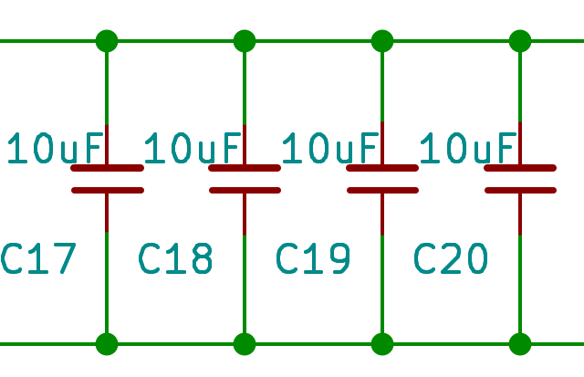
It is always a good idea to stick to the same style through the whole schematic. It is also a good idea to use symmetry as much as possible. For example if you have 4 capacitors that fulfill cca similar function they should be arranged in the same way.
Every engineering drawing should have a metadata section or a title block. Even if you will be the only one to see the schematic, you should fill at least the basic stuff. At least the project name and ideally the revision and date. The idea is that if you stumble upon some version of the schematic in the future, you should be able to find out what project and what version it is.
You should have the right amount notes in your schematic and the notes should be just enough specific. As mentioned earlier, you can use links and/or hierarchical sheets to provide more information without risking to clutter your schematic.
There are two types of notes that you want to use. First are free texts and they are typically used for logical block descriptions or for notes that are related to more components. i.e. you can have note describing power inputs accepted by your power source, differential pair routing requirements, etc.
The second type of notes are notes related to a certain component. Many design suites allow you to add fields to the component and usually they can be visible or invisible. You can include part numbers, internal part numbers, any additional requirements,… And you can choose whether the note is visible or not. The invisible note will not be printed with the schematic but can be included in bill of materials or any other project documentation.
Fields in KiCad (with added invisible field internal_link):

Almost every IC needs at least one decoupling capacitor – and usually much more. There are two ways where to put them. You can either put them near the IC near the pin that they should be decoupling or you can position them all away into a separate block with all the decoupling capacitors. There is no right way how to do that and there has been many heated discussions about this topic.
It is up to you to choose the way that suits you but remember to be consistent. And if you put them away from the IC make at least an invisible note for which IC and pin they are.
Near the IC:

Apart in a separate block:

All rules mentioned in this tutorial are more guidelines than strict rules. No design suite will enforce them, maybe there will be some warnings but hey, who cares about warnings anyway? On the other side you should be aware of them and you should have a good reason if you choose to not follow them.
Sometimes you need to connect two nets but you want to do it in a specific way. One example is the trace antenna connected to the ground. The point of the antenna is to be a trace of a specific length, width and shape. If this antenna should be connected to ground on one end, it would make the whole antenna become ground.
The net tie is in fact a simple component used just to connect two (or more) nets without combining them into one net. So with the antenna example you can have an antenna net and connect it to ground at the specific point you need.


