A few years ago, when discussing signal integrity, the focus was generally on models and software. However, nowadays, engineers are gradually starting to pay attention to the impact of PCB materials on high-speed circuits.
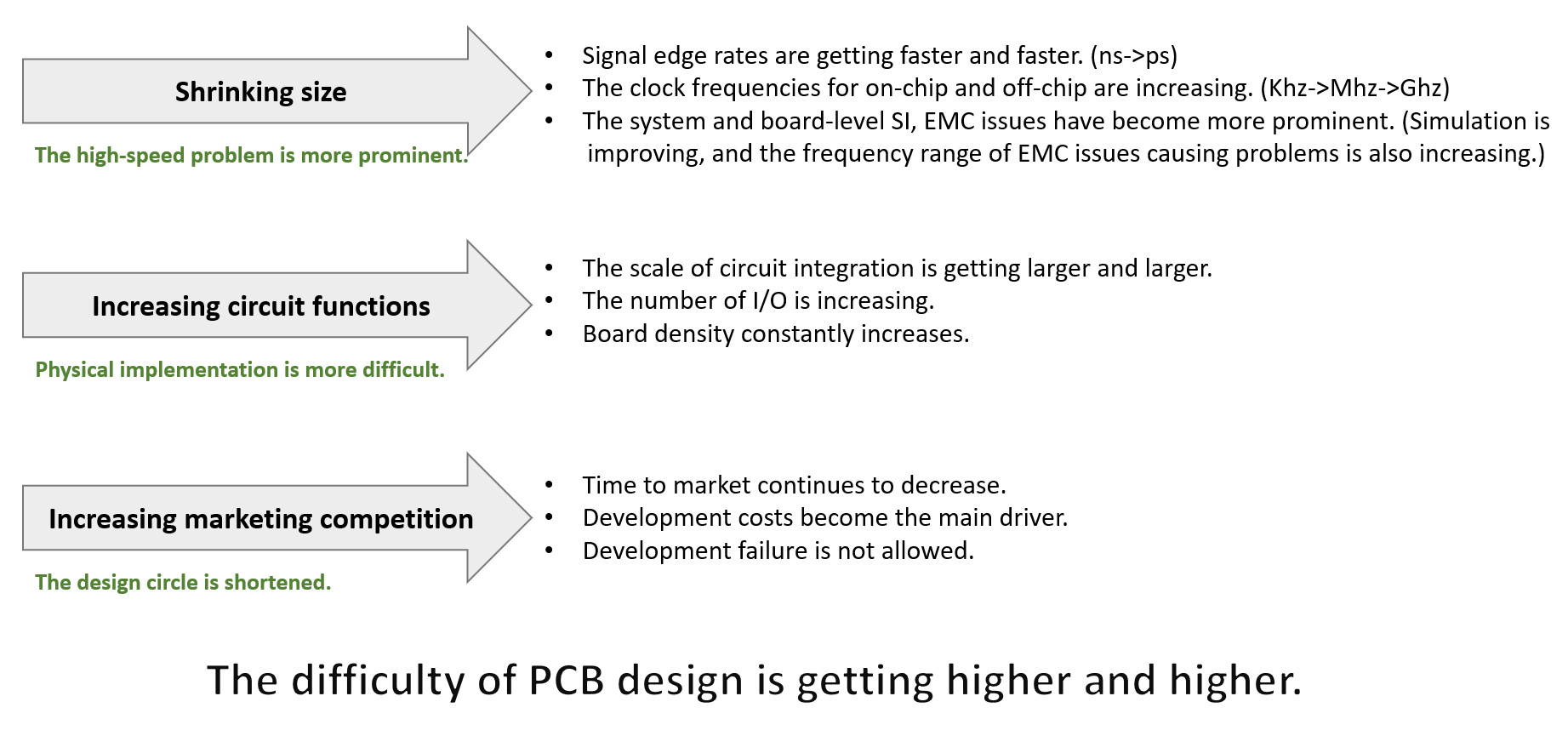
With the increase in data rates, as the frequency of the signal increases, its energy attenuation also becomes larger, as illustrated in the following diagram:
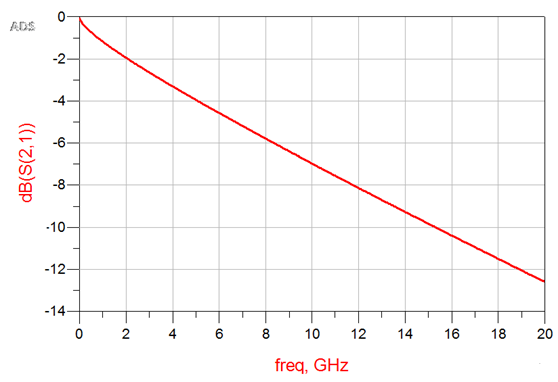
Simulation can be used to analyze the different effects of various materials on the signal. For example, by scanning different dielectric loss angles (Df, different dielectric loss angles represent different material types), different loss results can be obtained, and further analysis can determine whether it meets the design requirements. The figure below shows the results of loss simulation for different PCB materials (Df,):
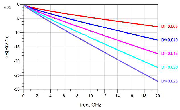
From the above diagram, it can be observed that the range of dielectric loss tangent (Df) is 0.005 to 0.025. The higher the Df value, the greater the attenuation. By analyzing the eye diagram, it is also evident that a higher Df value leads to a smaller eye-opening, as illustrated in the following diagram:
The analysis for the dielectric constant (Dk value) is similar, but the dielectric constant primarily affects impedance. Dielectric constant and dielectric loss tangent are two fundamental properties of a dielectric material, both vary with frequency, as shown in the following screenshot of a material's datasheet:
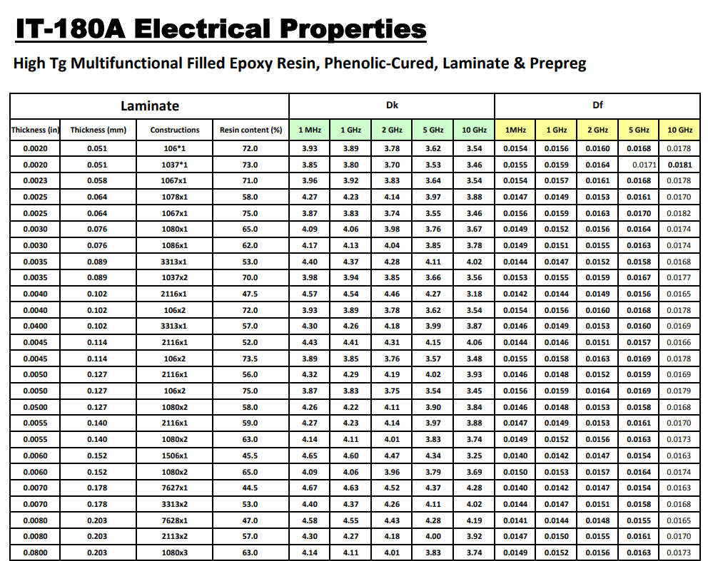
From the information provided, it can be observed that the parameters (Dk and Df) vary for different frequency points. However, the datasheet only provides data for five frequency points for each material. In many cases, datasheets may provide data for only one or two frequency points. So it is evident that using such limited data for calculations or simulations may result in inaccurate results. As shown in the following diagram, we can see a significant difference between the simulation results using the manufacturer's provided raw data and the test results obtained for a specific material:
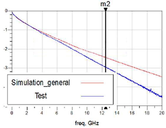
It’s understandable that obtaining such results is understandable since material parameters may not be accurate. After conducting testing and simulation to extract PCB material properties, the generated curve is depicted in the following diagram:
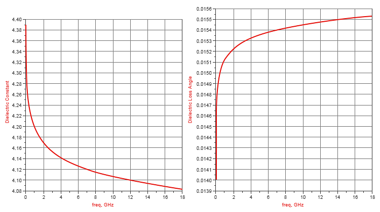
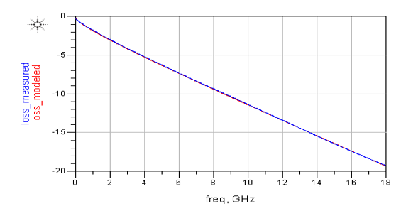
On the left side is the dielectric constant, which clearly decreases as the frequency increases. On the right side is the dielectric loss tangent, which increases with higher frequencies. By using the extracted material parameters for simulation (simulating a different transmission line), it is possible to obtain simulation results that closely match the test results, as shown in the following diagram:
Indeed, not only does the dielectric constant and dielectric loss tangent impact signals, but the roughness of the conductor (typically copper) can significantly affect the signal.


