board
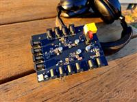
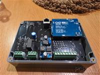
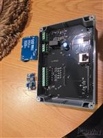
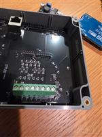
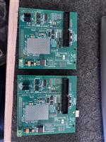
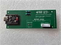
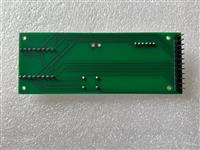
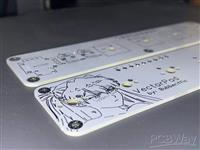
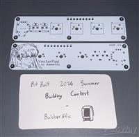
Clear and organized component placement. Routing is neat with minimal unnecessary trace crossings. Adequate separation between functional blocks. Silkscreen markings are readable and properly positioned. Design follows most standard PCB layout practices.
Aug 07,2026
30 viewsReport item
- Comments(0)
- Likes(0)
Upload photo
You can only upload 5 files in total. Each file cannot exceed 2MB. Supports JPG, JPEG, GIF, PNG, BMP
0 / 10000