Hello, readers welcome to the new post. In this post, we will have a detailed look at How to Design PCB in Proteus. PCB stands for the printed circuit board. It is the circuit board over which different types of projects and circuits are assembled for practical usage and applications. Nowadays it has become the very basic part of an electronic industry where it employed for the creation of projects and devices such as a computer, mobiles, laptops, boards of all these devices are assembled through PCB over which different components used in the circuit are assembled.
The most important part of the design of PCB is a very critical and main part of the practical use of PCB in any device and project creation. If you did not create an accurate design then there will be difficult for you to make practical creation of your projects. In this tutorial, I will teach you how you can design your PCB in Proteus software that is a very simple and easy tool for you to design any PCB design. So let get started.
Introduction to Proteus
- Proteus is electronic designing-based software that used to make the design of any project and circuit before making it practical.
- There are numerous options available in this software that helps to design PCB and practical learning of different types of design tools.
- This software is designed by Labcenter electronic. It helps to create a 2 D circuit design according to circuit configuration.
How to Design PCB in Proteus
- Let us make our design in proteus of PCB. First of all, open the software in your computer after the installation of this software.
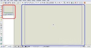
- When you will run the software in your computer the interface shown below will be seen on your computer screen.
- Here is P and L option are exist fro that option we can select components used in our projects and in rectangle box of blue color we will make our Projects circuit.
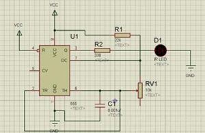
- To make PCB design in the proteus we will construct the circuit shown below that thirty-eight-kilohertz frequency generator configuration and using 55 timers integrated circuitry.
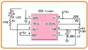
- The elements used in this circuit are 555 timers, four seventy kilo resistance, twenty-two-kilo resistance, and ten-kilo resistance, with LED and 0.001 microFarad capacitor.
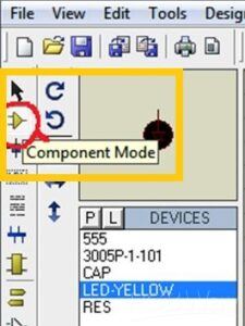
- For selection, all these components used the move to Library tab and choose Pick device tab shown in below figure.
- Here in the figure, you can see the component mode from which all components can be selected.
- From the above-shown library, we can get the required elements used in our projects. When you click on any component it will be automatically added to the working area.
- The placement of the component in the proteus working area is that when you drag the component pin towards another component it will make a connection to it.
- In the below figure you can see the oscillatoror circuit that we are going to design in our proteus. all components are selected in proteus according to step mention above and are linked to each other to make a circuit.
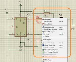
- to make changes in the component parameters linked to the circuit just press right at that component then the properties box will open through which we can change the values of that component.
PCB Layout In Proteus
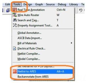
- Now come to the main point that is PCB design proteus. For this we will use above mention circuit. To design PCB in proteus there is an ARES designing tool is exist that we will use to design PCB.
- To use this option after running your software move to the tools option shown in below figure then press at the netlist to Ares.
- When you press at netlist Ares will see this window.
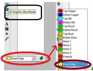
- After that we will create our design through the usage of 2D graphics box Mode,
- Press at the select layer and now choose board edge.
- After that now construct the box shape in the working area. After that press mouse button then the color of green line will turn in yellow.
- Now we can construct our circuit in that rectangle box.
- After that press at the element and change its location if needed through the use of the rotation tab after that put it in the working area.
- When you put all elements in the working area make a configuration of all these elements.
- the location of any element can be varied through pressing at the selection mode and after that chose the element and move it to the new location.
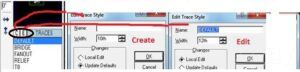
- After that link, all the elements of circuitry, Choose trach option and now we can vary the track width through choosing C or E option.
- Through choosing these tabs there will be a new screen will open.
- Choose the width of the screen according to layout of PCB circuitry.
- After that link all elements used to press at the elements at endpoint there will be green colored line that will show move this line to another component where you have to link.
- After making link green line will automatically diminish.
- For a single layer, PCB designing put all elements of circuit at one side and make their links at the other side.
- For two-layer PCB connection and interlinking of all components can be made at both sides.
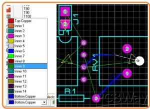
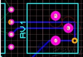
- The direction of elements used isá shown in white color arrowheads joints through green-colored lines and track shown through blue color lines.
- If there is any fault exist in our design will show in red color circles.
- To avoiding any fault, we can vary the track path. In the case of 2 layer PCB, we can vary track amongst layers through double-pressing the left button.
- The oranges color circle is shown vias exist among the layers.
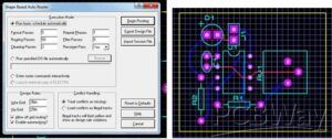
- There is an auto-router toll exist that can be used to configure the track by own.
- We can select auto-router display then the display will show that has all functions which we have to use. For routing press, at routing tab, it will start function.
- Red color track seen shown at upper portion and the track of blue-colored shown at lower portion among layers. It is 2 layer PCB.
- When tracking is completed save the project in the similar file that we saved in proteus.
- We can also select a three-dimensional display for a final look of our project.
- We can analyze all joints of elements angles placements and other parameters.
How to Print Layout
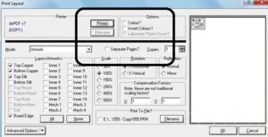
- This is the last step of our design configuration. TO perform this move to the output tab and press at the print button.
- Here you can see the print window. Here is numerous properties exist like mode, path, scale, etc.
- Here are four options exist that are solder resist, SMT mask drill plot ant artwork.
- Through artwork, the yellow-colored module assigned can be print.
- One thing retains in mind that for lower copper sheets there is necessary to choose mirror reflections.
- So numerous printouts of our design can be taken.
Note: The content and the pictures in this article are contributed by the author. The opinions expressed by contributors are their own and not those of PCBWay.


