Flexible circuits can offer a number of advantages over rigid PCBs being not only very thin but can include connection systems and cables as one single assembly. They can also be formed into the housing or simply provide a very thin substrate. They generally consist of various layers, built up and bonded with epoxy:
· Top Coverlay
· Top Copper Layer
· Insulator
· Bottom Copper Layer
· Bottom Coverlay
· Stiffener
They are more difficult to design, features have to be large in size to ensure robustness and traces need to be curved to prevent stress fractures. They are not straightforward to develop using free tools, as they will lack certain features to manage the complexities; Coverlays, copper features used to ensure a rugged design and conductive patterns for items such as switches.
In this design, it has 2 copper layers with vias, soldered surface mount components, double switch contacts and nearly 1 meter long. The contact arrangement is designed to be used with a rubber membrane switch contact array with carbon pips. There are two sets of contacts per key in order for the processor to measure velocity. In the original part it has carbon coatings instead of gold plating to keep costs low, however, they can oxidise over time and stop working properly. The picture below shows a section of the original failed green flexible circuit from an instrument.

The switch contacts and FPC connector make the design immediately problematic for a low feature count CAD tool, because the Coverlay has to be excluded from the switch contact area.
An overview of the general characteristics and a concept design is first created. It is important to decide on a large and robust feature size for tracks, vias and component pads.

First assessment involves the choice of connector, in this design a rugged 1mm pitch Molex 522072460 24Way top contact gold plated connector is chosen. The construction and stack up of the layers is critical for the connector, as it has a very tight tolerance. The rest of the design will follow the stack up around the connector as it has a wide tolerance and keeping consistent stack up across the design ensures a cost effective design and manufacturing process.

The free version of DesignSpark PCB is an excellent tool for designing PCBs, it has a number of limitations however when working with Flexible PCBs but they can be overcome with careful workaround and use of a Gerber file editor such as “Gerbv” available on the Linux platform. The basic limitation for managing
· Inability to exclude solder resist in specific areas of PCB symbols, thus limiting it’s use for the coverlay.
· Unable to place additional fixed copper elements that are not pads in PCB symbols to support ruggedisation features such as spurs
· Unable to prevent generation of paste mask for PCB pad symbols (for example for FPC connectors & switch contacts)
· Deal with pads on Top and Bottom side copper layers
· Unable to omit vias from the soldermask output file in order to use it as a coverlay that fully insulates a layer
· Limited to one documentation layer, having more than one could be used to generate various manufacturing drawings
· Fixing holes are not “plain” and are always have copper
Workarounds for these properties are managed carefully:
· Documentation layer is used to create aperture areas for the Coverlay that is merged with the solder mask during Gerber output.
· A separately saved version of the PCB is modified with vias removed and board outline replaced with two outlines for the stiffener regions.
· For adding additional unconnected copper layers on FPC connectors to achieve proper stack up, the FPC component pads are copied and reassigned to the other copper layer.
· A different tool is used for engineering drawings, such as Visio.
· A Gerber editor is used to remove solder paste mask features for FPC & switch contacts, a great tool called Gerbv” that runs on the Linux platform is used here.
It is vital that your own library of components is created. If using component library databases such as SamacSys copy the component parts you need and make your own with the necessary modifications.
The switch contact has pads and a documentation layer to define where the Coverlay aperture lies. In this example it is important that the switch membrane pads do not catch the edge of the Coverlay when operated as they may result in a bad connection.

The FPC is created with the documentation layer showing the exclusion of Coverlay film plus a copy of the top copper layers if required to meet a defined stack up.

Create fixings and other components used in the design as you would in a normal PCB. For stack ups that have a deep Coverlay, it may be necessary to define and exclusion area using the documentation layer as in switch components so that the body of the component can sit flush to the film and not lift the legs off the pads. Many small power diode packages have this property and can cause re-flow soldering issues.


In above examples, it is important to remember that the Coverlay is not just to resist solder but to provide mechanical strength to prevent tracks and pads from peeling off when flexed. The components above are defined for a flexible circuit in a “static” application, ie. flexed only during final assembly. For applications that have regular flexing then other measures such as adding spurs to pads to help pin them down under the Coverlay is necessary. This can be done by adding tracks manually to the design.
The design is now undertaken after entering the schematic. Making connectivity mistakes with Flexible Circuits has a very high cost associated as they are extremely difficult to rework or modify. Even for simple circuits, it is therefore strongly recommended to not move directly to a layout but create a linked schematic too so that all the circuit nodes and design rules can be verified.
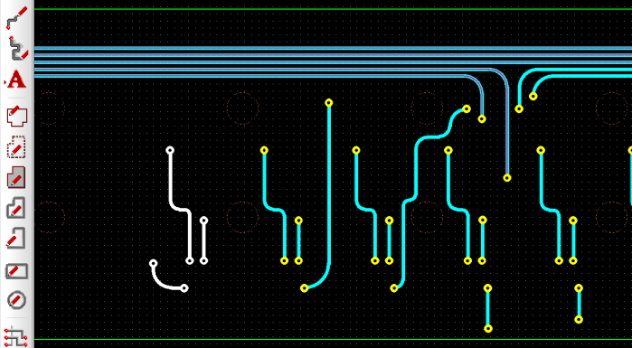
In an excerpt for the design below, curved traces, large clearances and features are used to ensure robustness.
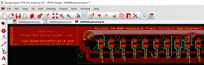
In this particular design, placement of components and fixing was notably painful, requiring tolerance of +/-0.05mm across the 1 meter length. The underlying metalwork, fixings and placement of switches is critical to ensure that the mechanical sub-assemblies fit correctly and do not affect the playing experience or missing notes!
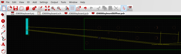
It is essential to create a copy of the PCB that has two board outline regions defined for the Stiffener regions and a soldermask with the vias removed. This was done by using “Save As”, once system and relative origins were set to a known fixing point on the PCB. In this case the bottom left fixing point on S1 was chosen and marked accordingly.
As the Coverlay data is generated from the soldermask output (with documentation layer merged) and the via holes are generated at same time. It is necessary to remove the vias and their pads somehow. The process of removing the unwanted vias on the derived design is then performed manually as shown below.
Once completed the “child” design is minus any via holes and the two stiffener regions can be seen as separate board outlines.
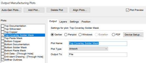
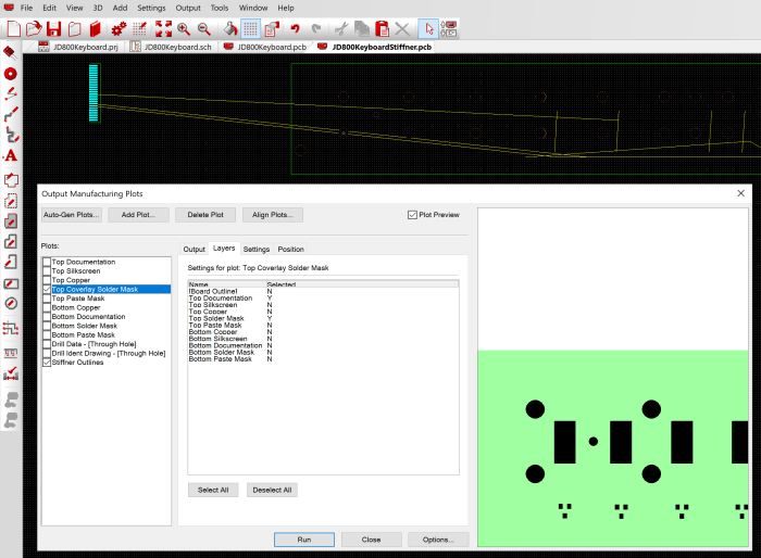
The next step is to create manufacturing information for the Top Coverlay and Stiffner outlines.
The Top Documentation layer containing additional Coverlay aperture information is turned on for the Top Solder Mask. The Top Solder Mask is also renamed to “Top Coverlay Solder Mask” to avoid confusion and a new plot “Stiffener Outlines” is created that is simply the board outlines.
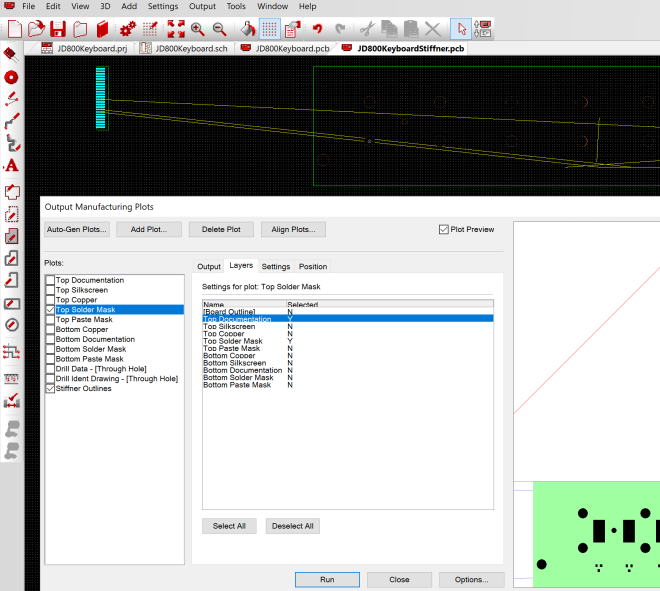
It can be seen from the preview that the Coverlay is now generated correctly.
In the original board layout, generate the remaining manufacturing Gerber files using the normal methods in accordance with your designed stack up and fine naming convention.
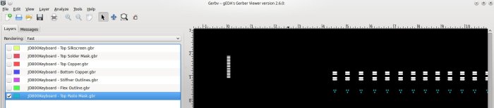
It is now time to edit the Solder Paste file and check the generated files in a Gerber file viewer. First load the files into Gerbv and check alignment of the layers and that they do what you need represented.
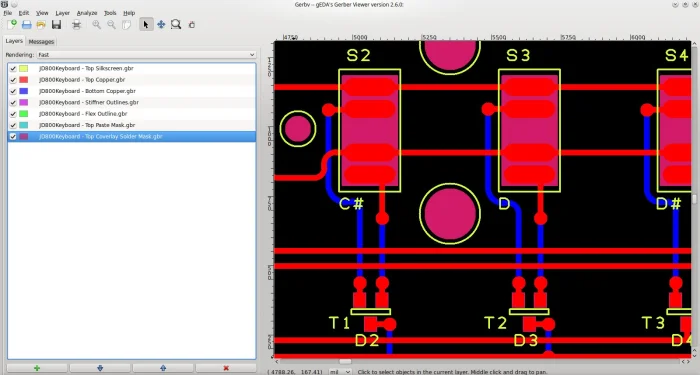
The hole placements can be checked too, simply load them into the viewer. Also a good idea to confirm that the via features are missing from the top and bottom Coverlays.
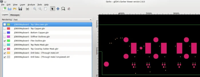
Select the Solder Paste Mask and delete the FPC and switch contact elements from the design.
It is done!
Gerbv now represents the manufacturing CAD data as you want it. All that is required now are the drawings that describe the characteristics, stack up and dimensional details. It is vital to represent a picture of what you require so that the essential properties may be checked at the factory by QA personnel.
Copyright © 2021 Super Synth Projects, Guy Wilkinson.


