


Mkbewe
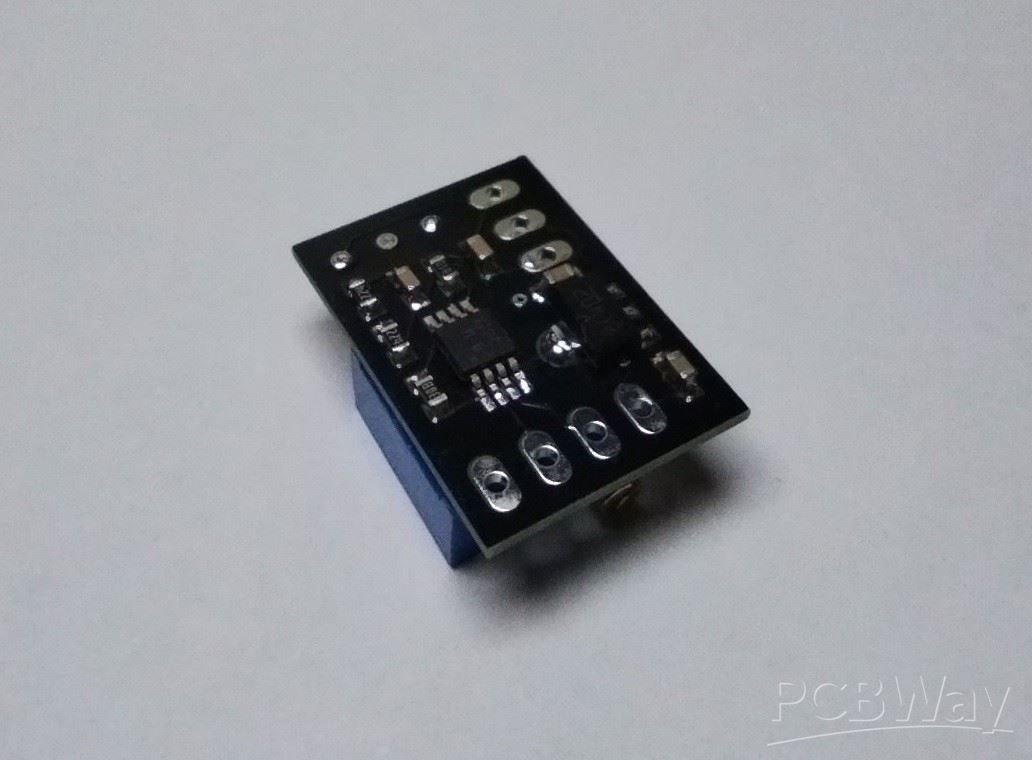
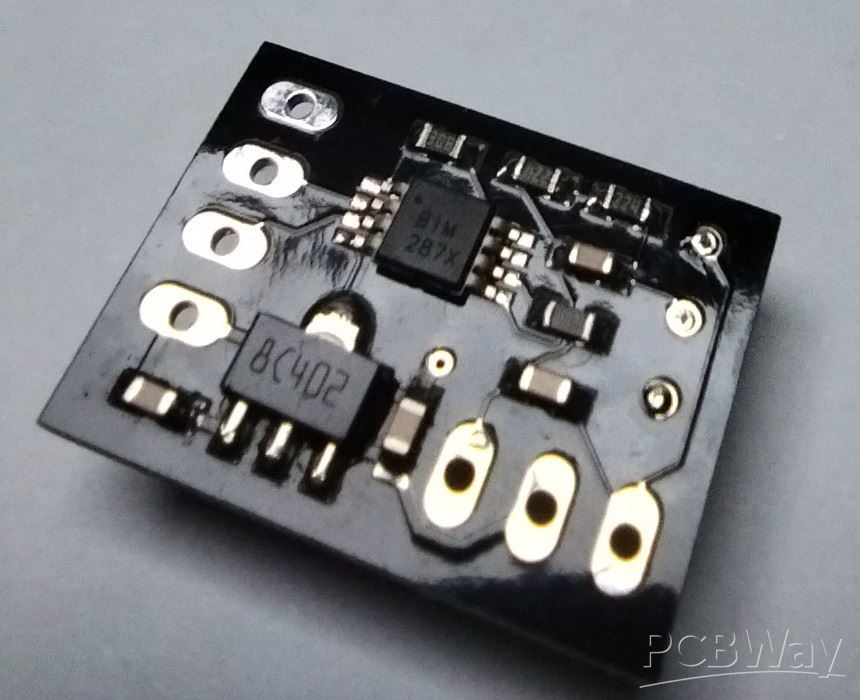
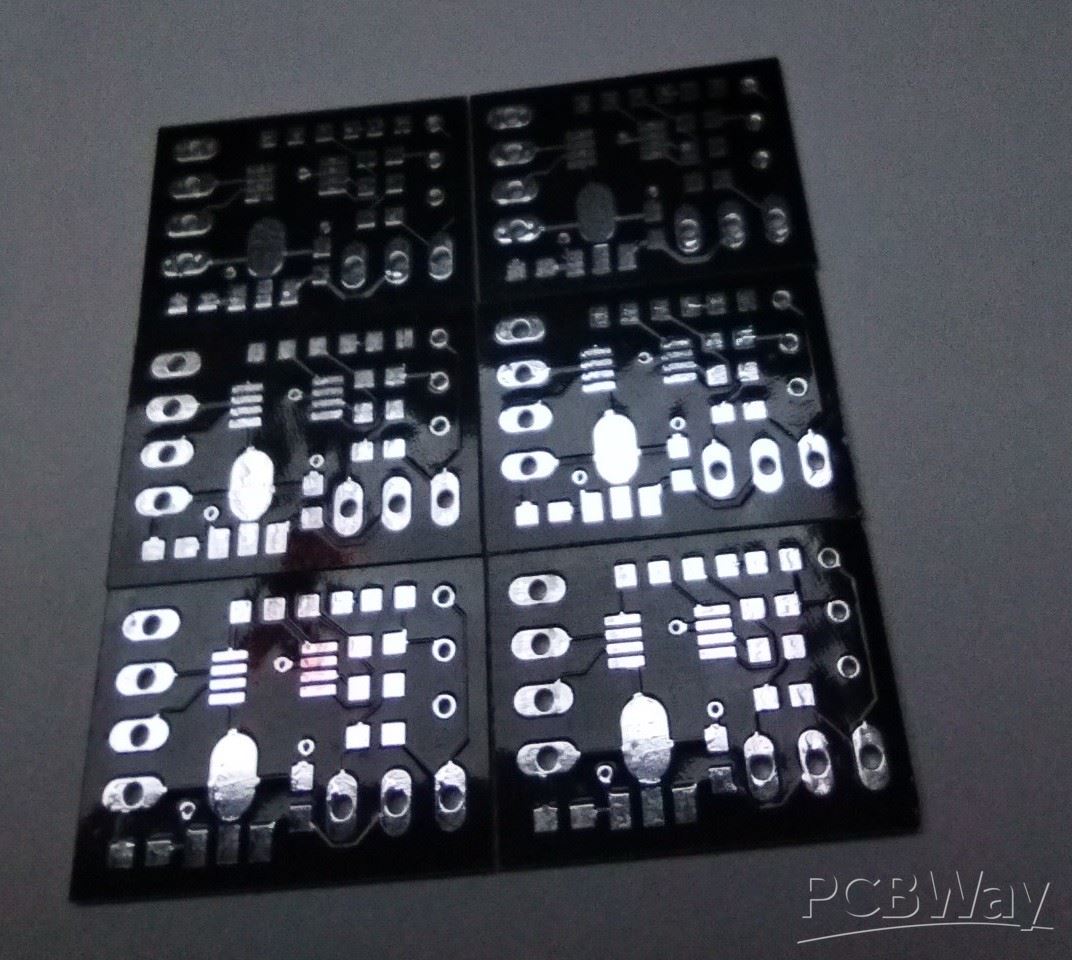
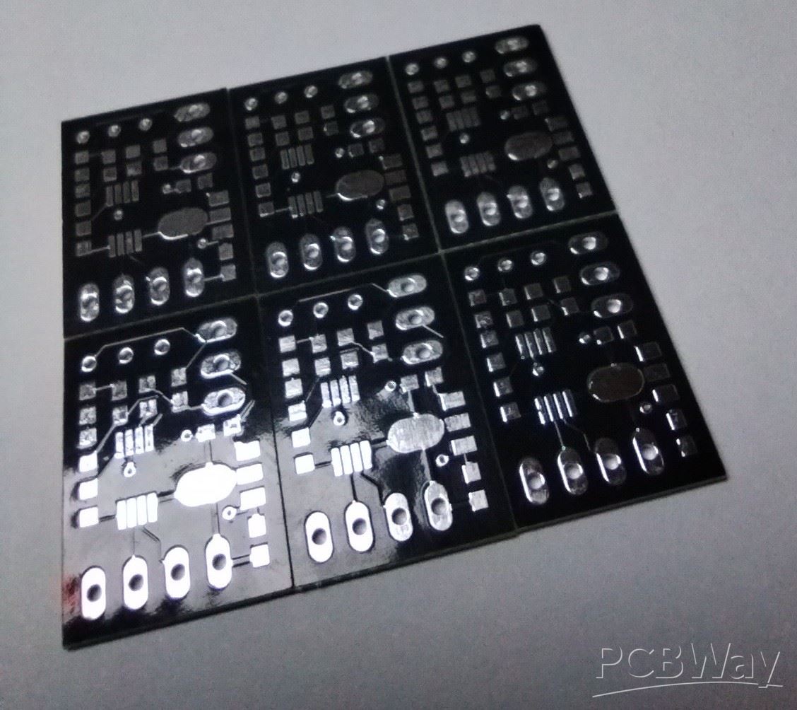
This is a PCB for a load cell amplifier. I tried to make it as small as possible because of limited space in a device where this pcb will work, I used just 6 mils trace width and same 6 mils spacing, anyway PCBway made it perfectly. No shorts, no broken traces, trace edges are smooth, solder mask is flawless, as well as vias and holes.

May 30,2025
241 viewsReport item
- Comments(0)
- Likes(0)
Upload photo
You can only upload 5 files in total. Each file cannot exceed 2MB. Supports JPG, JPEG, GIF, PNG, BMP
0 / 10000
You might like


