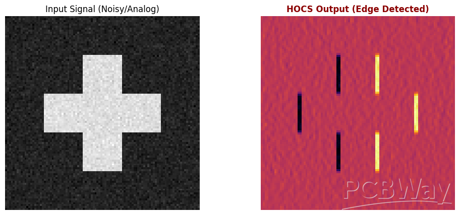
HOCS: Hybrid Optical Computing System - 4.14 TB/s Data Path
HOCS (Hybrid Optical Computing System) - 4.14 TB/s Zero-Heat Architecture
1. The Global AI Bottleneck: The Thermal Wall
The semiconductor industry is rapidly approaching the physical limits of traditional copper interconnects. As modern AI accelerators, Tier-3/Tier-4 data centers, and high-performance computing (HPC) nodes scale, standard server buses convert an immense amount of input power into waste heat. This phenomenon, known as the "Thermal Wall," causes severe throttling and physically limits the bandwidth density achievable with copper wiring.
2. Our Solution: Beyond Silicon
HOCS is a next-generation hardware architecture designed to bypass these silicon and copper limitations entirely. Instead of pushing electricity through copper traces for heavy data payloads, we integrate a patent-pending 50nm CuO hybrid photonic data path directly into the computing pipeline. By routing data via light at the bus level, we achieve an unprecedented data throughput of up to 4.14 TB/s.
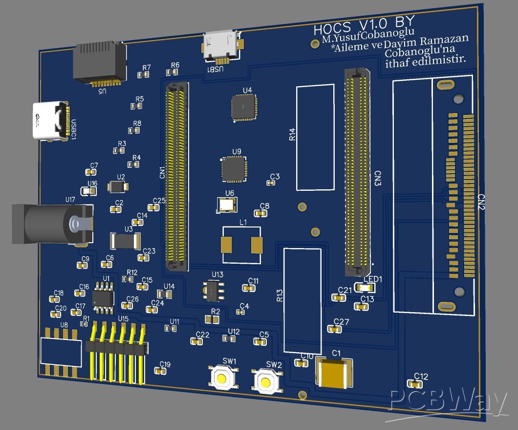
3. Hardware Architecture & Extreme PCB Demands
The HOCS Dev-Kit validation board is a highly complex, mixed-signal hardware driven by the Xilinx Kria K26 FPGA architecture. It interfaces with 400G PAM4 optical transceivers and high-speed laser drivers. This requires extreme PCB manufacturing capabilities:
- Complex Stack-up: A 6 to 8-layer stack-up using High-Tg FR-4 to guarantee signal integrity at multi-gigahertz frequencies.
- Impedance Control: Strict 85-ohm routing for PCIe Gen4/Gen5 data lines and 100-ohm routing for the optical transceiver loops.
- Surface Finish: ENIG (Electroless Nickel Immersion Gold) is strictly required to handle high-frequency routing and ensure reliable SMT assembly for high-density BGA components.
4. Performance & Physical Validation
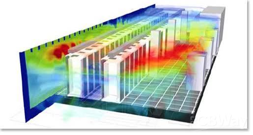
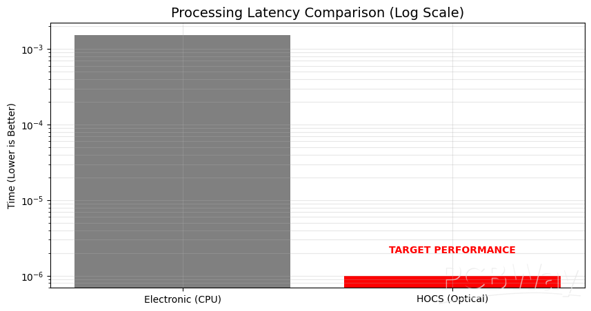
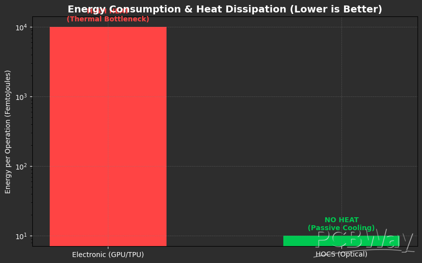
Our architecture reduces interconnect power consumption by 90%, practically eliminating heat generation at the bus level (a Zero-Heat architecture). Extensive Vivado and high-frequency simulations confirm our theoretical models against traditional electronic CPU/GPU bottlenecks.
5. The Team Behind HOCS
We are a dedicated team of hardware architects, photonics researchers, and FPGA embedded systems engineers who write code directly at the silicon level.
- M. Yusuf Çobanoğlu (Founder & Lead Architect): Directing the hybrid photonic architecture and hardware deployment.
- Mikail Yusuf Urğun (Co-Founder - Algorithms & Operations): Leading system-level algorithms and strategic operations.
- Mert Poyraz Akcan (Co-Founder - Photonics R&D Engineer): Specializing in optical data routing and thermal threshold optimization.
- Ali Ekber Şahin (Embedded Systems Engineer): Managing the Xilinx/FPGA programming pipeline.
- Muhammed Koç (Hardware Engineer): Responsible for Altium designs and high-speed multi-layer PCB routing.
- Mustafa Bayram (Integration Engineer): Executing PoC field testing and data center Rack-Mount deployments.
6. Why We Need PCBWay
Standard PCB fabrication is not an option for HOCS. We are applying for this sponsorship because PCBWay's proven track record in manufacturing advanced, impedance-controlled, and high-frequency boards directly aligns with the extreme tolerances our physical validation demands.
Apply for sponsorship >>- Comments(0)
- Likes(1)