Many DC-DC power chips provide a Remote-Sense function. However, many designers mistake it for an optional secondary connection and wire it directly near the power module's local output. This setup effectively renders remote sampling useless. During the debugging phase, various anomalies may occur: while the local output voltage of the power module appears normal, the supply voltage at the BGA core experiences continuous droop; the power supply may exhibit audible noise, Loop Stability degradation, and severe output voltage ripple fluctuations.
Remote-Sense is not a redundant line, but a Kelvin Sensing line used to measure the actual voltage at the load. The main power path carries high load currents, whereas the Force & Sense architecture ensures the Force & Sense signal paths remain isolated. Because the Force & Sense sensing line features high input impedance with minimal input bias current, it avoids the significant voltage drops present along the power delivery path, thereby measuring the load voltage more accurately.
Modern processor core supply voltages continue to drop, with typical values around 0.8V or 0.85V, while operating currents can reach tens to hundreds of amperes. Even with wide copper traces and dense via arrays on the PCB, inherent DC resistance remains in the copper foil, connectors, vias, and BGA fanout regions along the power path. As large load currents pass through these impedances, a noticeable IR Drop occurs.
For example, assume a DC-DC module has a local output voltage of 1.0V, and the total equivalent resistance of the power path from the module to an FPGA's BGA power pins is 1.5mΩ. Under a 100A load current, the voltage drop
VIRDrop = I × R = 100A × 1.5mΩ = 150mV.
Thus, while the local output stays at 1.0V, the actual voltage at the FPGA BGA pins drops to approximately 0.85V due to IR Drop along the copper, connectors, vias, and BGA fanout.
If the sampling point is placed locally at the DC-DC output, the Feedback Loop can only detect the local 1.0V rail. The Feedback Loop remains unaware of the 0.15V lost before reaching the load. For low-voltage core supplies, the allowable voltage tolerance is tight, depending on processor, FPGA, or ASIC specifications. Such voltage degradation caused by IR Drop leads to full-load crashes, frequency throttling, and inadequate timing margins on high-speed interfaces.
Remote-Sense resolves this problem: by routing the Remote-Sense sampling line directly near the load chip's power pins, the system detects the true voltage at the load. When the detected load voltage falls below the target, the Feedback Loop increases the power stage output to compensate for the IR Drop along the power delivery path.
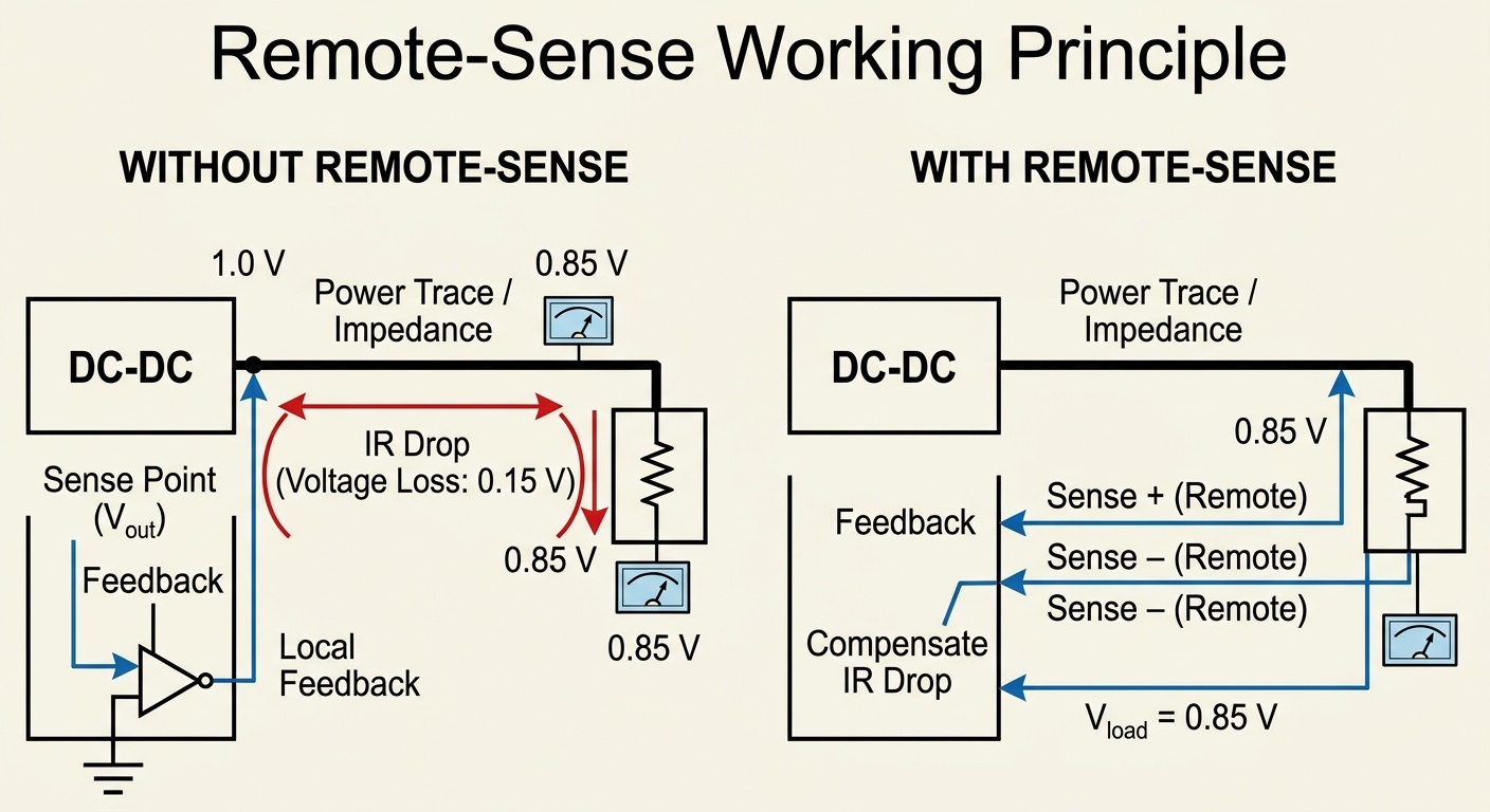
(Remote-Sense Working Principle)
At its core, Remote-Sense relies on Kelvin Sensing principles to segregate the high-current power path from the voltage detection line.
The power path delivers actual energy to the load and requires sufficient copper width, copper weight, and parallel vias to lower impedance. Because this pathway carries the full load current, it inevitably suffers from IR Drop.
The Force & Sense sensing line has high impedance and carries only a tiny input bias current. According to V = I × R, because the current flowing through the Force & Sense sensing line is negligible, its trace resistance creates virtually no voltage drop compared to the high-current power line. Consequently, Kelvin Sensing measures the electrical potential at the load with high accuracy.
The power converter's internal Feedback Loop continuously measures the error between the sense voltage and an internal reference voltage, adjusting power delivery to compensate for PCB power losses.
For ICs featuring Differential Sensing, both VSENSE+ and VSENSE- must be fully connected as specified in the datasheet. Incorrectly connecting only a single sense line may cause reference errors or disable remote sampling altogether.
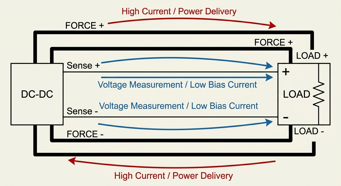
(Kelvin Force/Sense Schematic )
Remote-Sense is far more than a simple jumper trace. Sampling point placement, routing methods, Noise Isolation, filtering, and Multi-Load Topology configurations all impose strict constraints. Improper implementation fails to compensate for IR Drop and risks introducing high-frequency noise into the Feedback Loop, inducing output fluctuations, degraded Loop Stability, or audible squealing.
VSENSE+ and VSENSE- must be routed using Differential Pair Routing, kept closely coupled in identical environments. Avoid placing either trace near SW Nodes, clock lines, or other noisy sources, and never run them parallel to power switching nodes over long distances. Adequate Noise Isolation is essential to prevent interference.
If the two traces experience different distances to noise sources, varying Ground Plane Reference structures, or unequal surrounding copper, external interference couples unevenly into the lines. This asymmetry converts into differential-mode noise, directly corrupting the Feedback Loop.
Therefore, the main objective of Differential Pair Routing is not simply maximizing line width, but ensuring both lines share a symmetrical, low-noise environment with effective Noise Isolation, minimal loop area, and a solid Ground Plane Reference.
Input filtering and Decoupling Capacitors must be placed as close to the chip power pins as possible to lower the high-frequency current loop impedance at the load.
The core principle of Remote-Sense layout is: The sense point must represent the true voltage received by the load, not an intermediate node along the power path.
Never place sense points arbitrarily along intermediate nodes or directly on power copper pour for layout convenience. Even if schematics correctly define Differential Sensing, improper Sensing Point Placement on the PCB invalidates the feature.
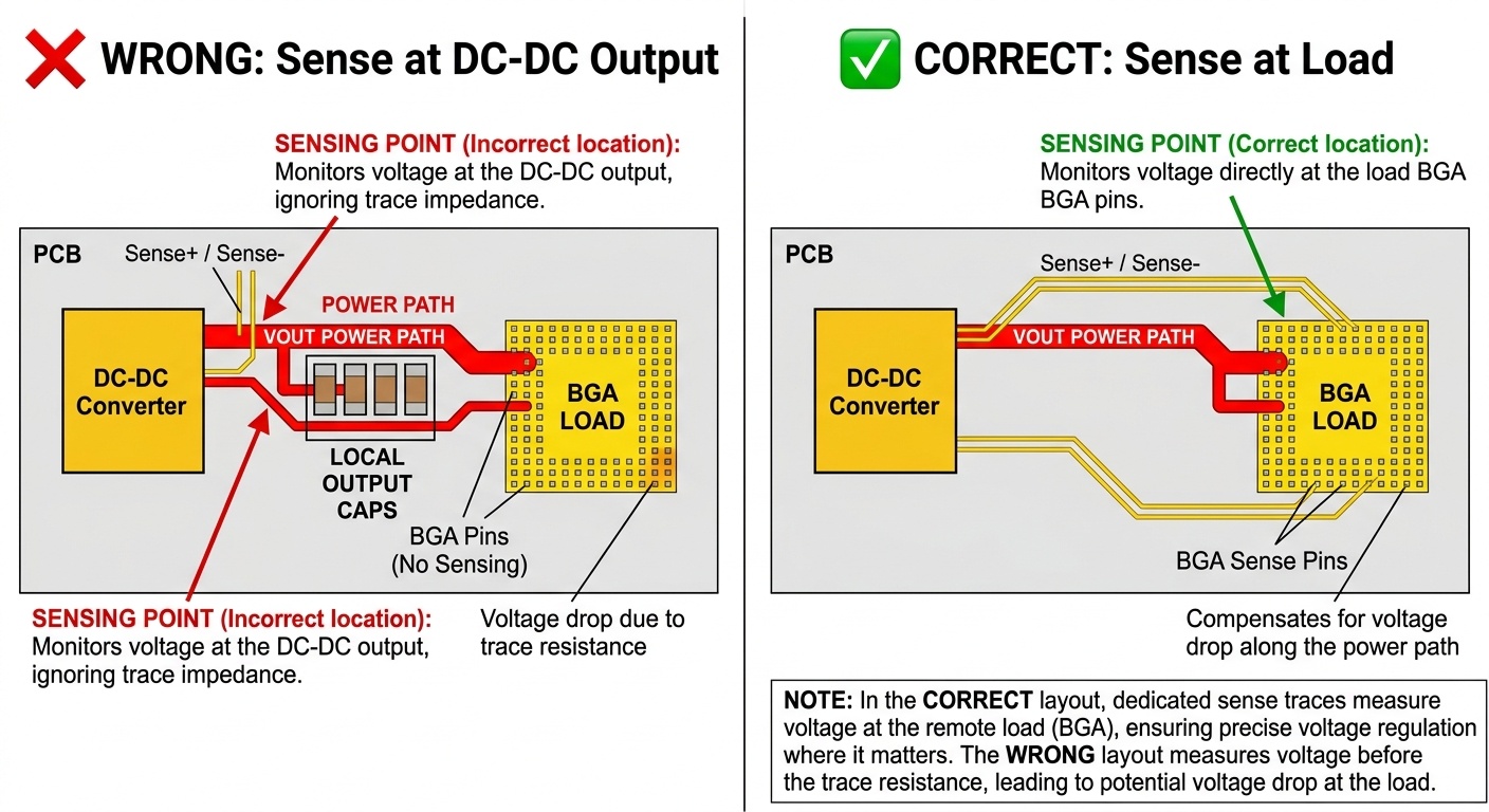
(Remote-Sense PCB Layout)
Sense traces often traverse long PCB paths, making them vulnerable to high-frequency interference from switching SW Nodes, DDR buses, clocks, and high-speed traces. Proper Noise Isolation helps, but if high-frequency noise reaches the sensing node, it induces output jitter and degrades Loop Stability.
For long sense traces or noisy environments, place an RC Low-Pass Filter near the sense pins according to datasheet recommendations to suppress coupled switching noise.
Some IC manufacturers recommend an RC Low-Pass Filter consisting of tens of ohms in series and nanofarad-range capacitors. However, specific R and C parameters must strictly follow vendor datasheets and be validated through Loop Stability testing rather than using generic values.
Note that an RC Low-Pass Filter introduces an additional time constant, requiring evaluation regarding its impact on loop bandwidth, Transient Response, and overall stability.
When a single power rail supplies multiple BGA devices, a Multi-Load Topology must not place the sense point at a random common node or simply at the load closest to the converter.
In a Multi-Load Topology, evaluate system voltage tolerances, load currents, and power path drops to position the reference point at the most voltage-sensitive load experiencing the highest drop.
For example, in a chain of DC-DC -> Load A -> Load B -> Load C, if Load C has the tightest tolerance and highest line drop in this Multi-Load Topology, connect the sense reference point directly to Load C's supply pins. This ensures the loop prioritizes the voltage margin of the critical load, while closer loads are powered via the main power path without serving as feedback references.
If a design does not enable Remote-Sense, do not leave the VSENSE+ and VSENSE- pins floating, as a Floating Pin Hazard will disrupt feedback control.
For controllers relying on external sense inputs, a Floating Pin Hazard leaves input potentials uncontrolled, causing abnormal output voltages and potential device damage.
To avoid a Floating Pin Hazard, consult the datasheet. Devices supporting local sense mode typically require connecting VSENSE+ to local VOUT+ and VSENSE- to local GND. Always follow the manufacturer's specified wiring for local sensing, as internal architectures vary.
Remote-Sense is not a substitute for proper load-side decoupling and low-impedance Power Integrity / PDN design.
Remote-Sense primarily compensates for DC or low-frequency voltage losses along the power path. When a CPU, FPGA, GPU, or ASIC undergoes a fast step change, the Transient Response of the feedback loop cannot react instantaneously. During these events, Decoupling Capacitors and a low-impedance Power Integrity / PDN supply transient current and mitigate sharp voltage dips.
Therefore, comprehensive Power Integrity / PDN design requires integrating multiple strategies:
Remote-Sense, power path optimization, and Decoupling Capacitors complement each other rather than act as replacements.
If Remote-Sense is connected to a distant load without being properly configured or enabled, incorrect feedback compensation may drive the local voltage too high, triggering OVP / UVP Protection, instability, or exceeding maximum operating limits.
Always consult the datasheet to confirm:
If the sense voltage drops excessively due to open circuits or extreme line losses, improperly configured controllers may trigger OVP / UVP Protection to prevent overvoltage damage at the local output or undervoltage failures at the load.
Ultimately, Remote-Sense is not just about routing two lines to the load. It ensures the feedback loop accurately measures the actual voltage delivered to the load while maintaining reliable OVP / UVP Protection and preventing noise or parasitics from degrading system stability.l