High-speed analog-to-digital converter (ADC) PCB layout involves multiple design parameters, and their importance varies depending on the application. For high-speed ADC systems, the focus should not be on optimizing every routing detail, but on avoiding common design deviations and maintaining the overall performance of the signal chain. For a broader overview of PCB Layout principles, designers should also consider signal integrity, power integrity, grounding, and return paths as part of the overall design.
The exposed pad (EPAD), defined as Pin 0 by ADI, is the core pad located on the bottom of many integrated circuit packages. It typically provides the main grounding and thermal connection and serves as an important path for the internal ground structure. Some converters and amplifiers do not have dedicated ground pins, with their grounding function primarily relying on the EPAD. Therefore, EPAD design directly affects electrical connection stability and thermal performance and should not be overlooked in ADC PCB design.
The EPAD must form a reliable solder connection with the PCB to ensure both electrical and thermal connectivity. Poor soldering or insufficient contact can lead to abnormal grounding, inadequate heat dissipation, and even malfunction of the signal chain.
For reliable EPAD performance, three key aspects should be considered in ADC PCB design.
According to the device datasheet and overall thermal requirements, grounding and thermal copper structures can be added on the appropriate PCB layers. These structures should provide reliable electrical and thermal connections to the PCB ground planes, helping improve heat dissipation, particularly in high-power and multichannel signal-chain applications.
The bottom layer can also incorporate a corresponding grounding or thermal area when required by the device and system design. Depending on the application, this area can support grounding, thermal management, high-frequency decoupling, or mechanical positioning for a bottom-side thermal structure.
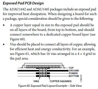
(exposed pad pcb design)
A large EPAD can be divided into multiple smaller areas using a cross-hatched stencil pattern or solder mask segmentation. During reflow soldering, solder paste distribution can vary across a large continuous pad, potentially resulting in uneven soldering, voids, or insufficient effective contact.
Proper EPAD segmentation helps improve solder paste distribution and create a more uniform and stable connection between the device and PCB, improving both electrical and thermal reliability.
Ground vias can be added to individual EPAD sections according to the device recommendations and PCB manufacturing requirements. Whether these vias require solder paste filling, epoxy filling, or other treatment depends on the via dimensions, pad structure, and manufacturing process.
For via structures that may allow solder paste to flow into the holes during reflow, appropriate via filling or solder mask treatment should be considered. This helps reduce soldering defects and improves the reliability of the EPAD electrical and thermal connection.
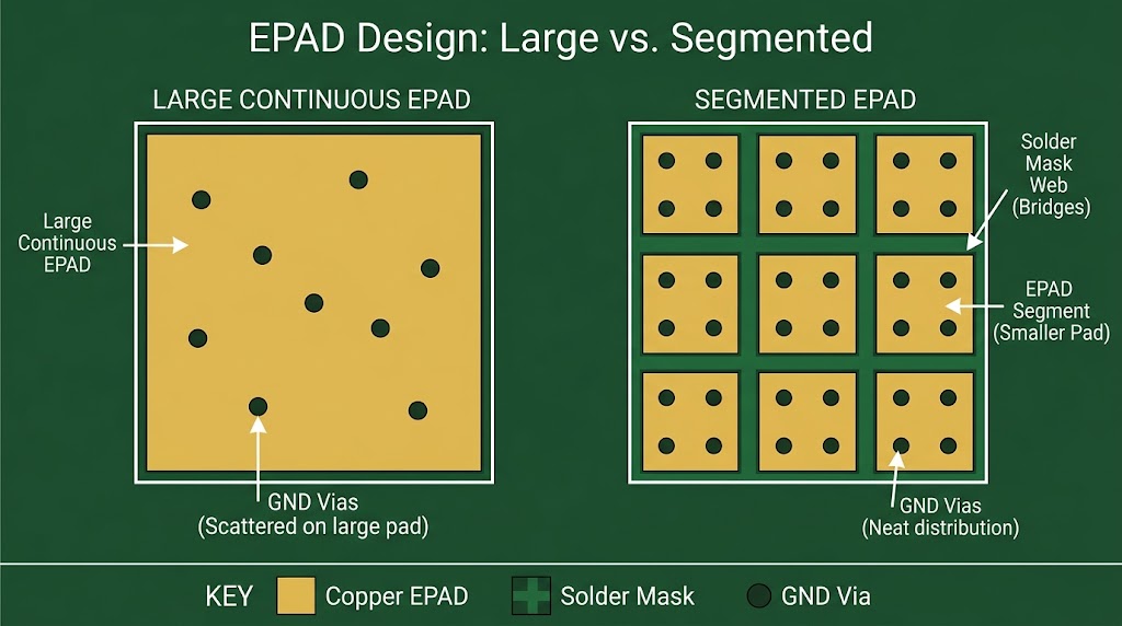
(EPAD design: large vs segmented)
The primary goal of PCB power decoupling is to reduce the impedance of the power delivery system (PDS) to ground. A common mistake is to place large numbers of capacitors with different capacitance values without considering their actual frequency response.
In practice, a large number of redundant capacitors is not always necessary. Carefully selecting capacitors based on capacitance, component type, package, and process characteristics can optimize PDS impedance while saving PCB space and reducing component cost.
Redundant capacitors can introduce layout congestion, additional cost, and potential resonance risks. They do not inherently violate PCB manufacturing requirements, but excessive or poorly planned decoupling can reduce overall design efficiency.
The performance of a capacitor varies with its package and construction. Even capacitors from the same supplier can have different frequency responses depending on package size, process, and component type.
Therefore, there is no universal frequency limit for capacitor decoupling performance. The effective frequency range depends on package size, equivalent series inductance (ESL), component characteristics, and the actual PCB layout.
If capacitor selection or placement is inappropriate, multiple capacitors can introduce additional inductive loops. Capacitors with different parameters may also resonate at specific frequencies, potentially increasing rather than reducing PDS impedance. Capacitor frequency-response characteristics should therefore be considered before placement and selection.
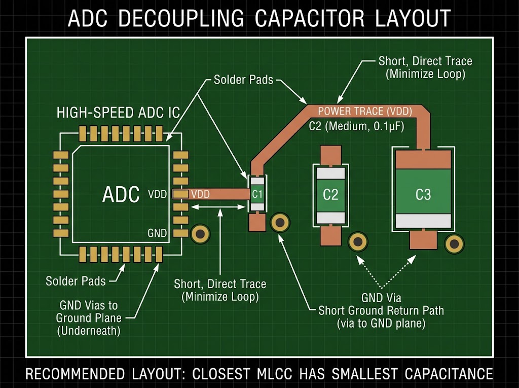
(ADC decoupling capacitor layout)
The effective decoupling range of discrete capacitors depends on their electrical characteristics and PCB layout, and there is no universal high-frequency cutoff. As frequency increases, package parasitics and ESL increasingly limit the high-frequency performance of discrete capacitors.
At higher frequencies, the intrinsic capacitance formed between PCB power and ground planes becomes an important part of PDS design. Proper stackup design can therefore complement conventional discrete decoupling.
A typical six-layer PCB stackup can be arranged as: Top Signal → Ground 1 → Power 1 → Power 2 → Ground 2 → Bottom Signal
In high-speed PCB design, keeping the dielectric thickness between adjacent power and ground planes relatively small, such as a typical range of 2–4 mil, helps increase plane capacitance and reduce the impedance of high-frequency current paths.
This optimization is achieved primarily through the PCB stackup and does not require additional components. The required stackup and dielectric thickness simply need to be specified in the PCB fabrication documentation.
For an eight-layer PCB, additional ground reference layers can be introduced while maintaining a small core-layer spacing, such as 2–3 mil. This can significantly increase the intrinsic plane capacitance, although the actual increase is not necessarily double. It depends on dielectric thickness, copper area, and the overall configuration of the power and ground layers.
Compared with simply adding more high-frequency discrete capacitors, stackup optimization can reduce component count and provide a cleaner high-frequency PDS structure.
The primary function of the PDS is to suppress voltage fluctuations caused by the dynamic current demand of the circuit. Low-impedance power and ground planes, combined with an appropriate PCB stackup, can reduce voltage fluctuations caused by rapidly changing currents.
According to V = IR, if the dynamic current is 1 A and the PDS impedance is 10 mΩ, the corresponding voltage variation is approximately 10 mV.
Optimizing the PCB stackup can extend the effective high-frequency low-impedance range, but overall PDS performance is also affected by power-plane integrity, ground-via placement, package parasitics, and local current-loop design.
Therefore, conventional low-frequency decoupling capacitors can be placed at key locations such as power-entry points, high-power devices, and surge-current devices. Combining different decoupling mechanisms can help optimize PDS impedance over a broad frequency range. Dense capacitor placement around every IC is not always necessary and may introduce unnecessary cost, space consumption, and resonance risks.
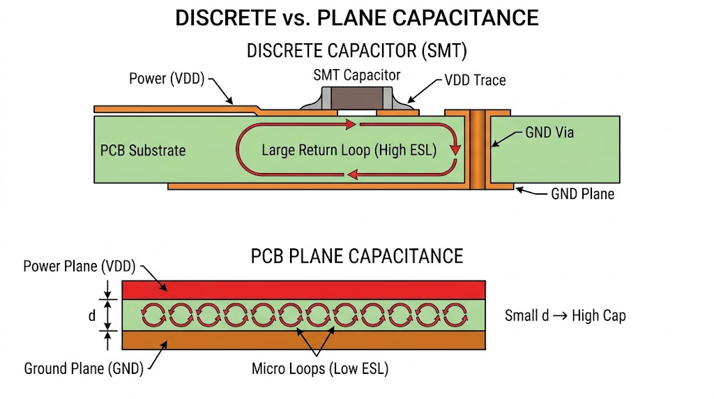
(discrete vs plane capacitance)
In multilayer PCB layouts, sensitive analog layers, including analog power, ground, and signal layers, can experience crosstalk when placed close to high-frequency digital layers. Because some noise sources are located directly above or below sensitive analog layers, this type of coupling can easily be overlooked.
Adjacent PCB conductor layers form parasitic capacitive structures, which can produce electric-field coupling under certain frequency and layout conditions. The actual coupling level has no fixed value and depends on factors such as layer spacing, dielectric thickness, copper area, routing length, signal edge rate, return path, and interlayer parasitic capacitance.
For example, if simulation or measurement confirms that a high-speed digital signal produces approximately 1 mV of interference at a sensitive analog node through layer coupling, this interference corresponds to about 2 LSB for a 12-bit ADC with a 2 Vpp full-scale range and about 8 LSB for a 14-bit ADC. In high-resolution ADC systems, such coupling can significantly reduce signal margin and system SNR.
Therefore, during ADC layout, the signal characteristics of adjacent layers should be carefully evaluated. High-noise digital layers should be kept away from sensitive analog layers where practical, while appropriate stackup, routing, and return-path design should be used to reduce interlayer coupling.
In ADC PCB design, there is no universal requirement to divide the ground plane into analog ground (AGND) and digital ground (DGND). The appropriate approach depends on the device manufacturer's recommendations, system partitioning, and current return paths. In many conventional applications, a continuous ground plane is preferable to unnecessary segmentation.
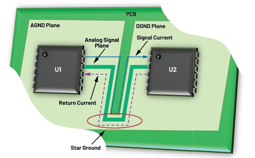
(Backflow Path)
Unnecessary ground-plane splitting can increase the inductance of current return paths. According to V = L(di/dt), higher return-path inductance increases transient voltage noise caused by rapidly changing currents and may also worsen the high-frequency impedance characteristics of the local power and ground network.
As ADC sampling rates increase, switching currents can change more rapidly, making parasitic inductance in the return path increasingly important. Therefore, a continuous ground plane should generally be maintained unless system requirements indicate otherwise.
The core of grounding design is functional partitioning and return-path optimization. By separating analog and digital circuits through appropriate component placement and controlling the return paths of high-speed digital signals, unwanted interaction between analog and digital sections can be reduced.
In many applications, proper PCB layout, a continuous ground reference plane, and controlled return paths can provide good grounding performance without physically splitting the ground plane.
Ground-plane segmentation may be considered when layout constraints prevent effective functional partitioning or when high-noise digital circuits and power buses cannot be sufficiently separated from sensitive analog circuitry.
However, a single-point AGND-DGND connection is not universally appropriate for every ADC system. The grounding method should be selected based on device characteristics, PCB return-path distribution, and overall system noise performance, with the device datasheet and system requirements serving as the primary references.
High-speed ADC layout should focus on the key factors that directly affect signal-chain performance rather than adding unnecessary design complexity. For system-level, module-level, and evaluation-board designs, a continuous ground plane can generally be preferred, with functional partitioning used to optimize return paths and reduce layer-to-layer coupling.
PCB assembly processes can also directly affect system performance. Manufacturing documentation should specify EPAD segmentation, via treatment, and other relevant assembly requirements according to the device and manufacturing process to ensure reliable solder connections.
Power decoupling should be based on accurate component selection and targeted placement. Combined with a PCB stackup that places power and ground planes closely together, this approach can improve high-frequency decoupling performance. Conventional low-frequency decoupling capacitors can then be used at appropriate locations to optimize PDS impedance over a broad frequency range.
For high-speed analog-to-digital converter applications, ADC PCB design should be adapted to the specific system requirements. A well-planned ADC layout should focus on device connectivity, power integrity, high-frequency impedance, layer-to-layer coupling, and grounding and return paths. By addressing these factors together, designers can improve the stability and overall performance of high-speed ADC systems.